
Intel Pentium 4 Processor in the 478-pin Package / Intel 850 Chipset Platform Family Design Guide

Memory Interface Routing
R
112 Intel
®
Pentium
®
4 Processor / Intel
®
850 Chipset Family Platform Design Guide
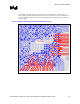
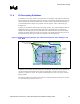
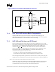
Figure 74. Rambus Technology Intel
®
MCH Breakout (Bottom Layer)
Bottom
Layer
Channel A
Channel B
6.2.1 Optimized Rambus RDRAM* Device Routing Rules for a
Four-Layer Motherboard Design
This section documents ONLY the routing guideline changes from the general guidelines outlined
in the Intel
®
Pentium
®
4 Processor in the 478 Pin Package / Intel
®
850 Chipset Family Platform
Design Guide.
General optimized routing guidelines that apply to Channel A and
Channel B
• Do NOT implement dummy VIAs on RSL signals routed on the top layer.
• RSL signals routed on the top layer need to be routed 25mils longer than RSL signals on the
bottom layer.