
Intel Pentium 4 Processor in the 478-pin Package / Intel 850 Chipset Platform Family Design Guide


Schematic Review Checklist
R
Intel
®
Pentium
®
4 Processor / Intel
®
850 Chipset Family Platform Design Guide 245
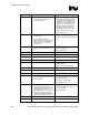
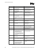
Checklist Items Recommendations Reason/Impact/Documentation
IERR# • Leave as a No Connect • Chipset does not support this signal.
• Asynch GTL+ output signal.
IGNNE# • Connect to ICH2.
• No pull-up required.
• Termination not required.
• Asynch GTL+ input signal.
• Refer to Section 5.4.1.2.
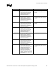
INIT# • Connect to ICH2 and Firmware Hub
(FWH).
• Voltage translation is required for this
signal to meet the input threshold
levels of the FWH.
• Termination not required.
• Asynch GTL+ input signal.
• Refer to Section 5.4.1.3.
LINT[1:0] • Connect to ICH2. LINT[1] connects to
ICH2 NMI and LINT[0] connects to
ICH2 INTR.
• No pull-up required.
• Asynch GTL+ Input Signal.
• Refer to Section 5.4.1.2.
LOCK# • Connect to MCH • AGTL+ common clock I/O signal
MCERR# • Leave as No Connect • Chipset does not support this signal.
• AGTL+ common clock I/O signal
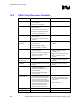
PROCHOT# • Terminate to VCC_CPU with a
62
Ω ±5% resistor near the
processor.
• Voltage translation may be required if
this signal is connected to external
logic.
• Asynch GTL+ output signal
• Refer to Section 5.4.1.1.
PWRGOOD • Terminate to VCC with a 300 Ω ±5%
resistor.
• Connect to ICH2.
• Asynch GTL+ input signal
• Refer to Section 5.4.1.4.
REQ[4:0]#
• Connect to MCH • AGTL+ source synch I/O signals
Reserved • Reserved signals must remain as a
No Connect.
•
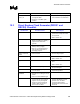
RESET# • Terminate to VCC_CPU with a
51
Ω ±5% resistor near the
processor.
• Connect to the MCH.
• AGTL+ common clock input signal
RS[2:0]#
• Connect to MCH • AGTL+ common clock input signal
RSP# • Leave as No Connect. • Chipset does not support this signal.
• AGTL+ common clock input signal
SKTOCC# • Connect to glue logic if pin is used. • Processor pulls this signal to GND.
System board designers may use this
pin to determine if the processor is
present in the socket.
SLP# • Connect to ICH2.
• No pull-up required.
• Asynch GTL+ input signal
• Refer to Section 5.4.1.2.