
Intel Pentium 4 Processor in the 478-pin Package / Intel 850 Chipset Platform Family Design Guide


Schematic Review Checklist
R
250 Intel
®
Pentium
®
4 Processor / Intel
®
850 Chipset Family Platform Design Guide
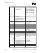
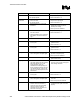
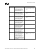
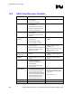
Checklist Items Recommendations Reason/Impact
Mult[1:0] • Connect to GPIO. • These pins determine the internal
PLL divider ratio in the DRCG.
Connection to GPIO allows software
adjustable PLLCLK and REFCLK
multipliers.
• The Intel 82850 chipset platform
supports 400 MHz (PC800) and
300 MHz (PC600) RAMBUS
operation only.
• The Intel 82850E chipset platform
supports 400 MHz (PC800) or 533
MHz (PC1066) RAMBUS operation
only.
ClkB/Clk • Connect a 39 Ω ±5% series resistor
near the pins. Connect 51
Ω ±5%
parallel resistors after the series
resistors through a 0.1 µF capacitor
to ground. Connect to RIMM*
connector.
• These signals should be terminated
with 28
Ω ±2% or 27 Ω ±1%
resistors to ground through a 0.1 µF
capacitor.
• This is the main clock (CTM/CTM#)
for the Direct RAMBUS channel.
• Refer to Section 4.3.4.
• Refer to Section 4.3.3.3.
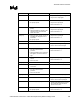
Global decoupling • It is recommended that a ferrite filter
with 2 capacitors (10
µF and 0.1 µF)
be placed near the part for both the
3.3 V planes. Capacitors should be
placed on the device side of the
Ferrite Bead. Ferrite bead should be
50
Ω at 100 MHz.
• Discrete capacitors are
recommended for all the
aforementioned decoupling.
• Cpacks are not recommended.
• This recommendation is to reduce
jitter and voltage supply noise for
the part.
• Cpacks will increase the parasitic
inductance of the capacitors, and
may require more capacitors than
specified above.
• Refer to section 4.3.4.