
Intel Pentium 4 Processor in the 478-pin Package / Intel 850 Chipset Platform Family Design Guide

Schematic Review Checklist
R
256 Intel
®
Pentium
®
4 Processor / Intel
®
850 Chipset Family Platform Design Guide
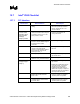
Checklist Items Recommendations Reason/Impact
SA Pins • Should be connected to VCC3_3 or
GND to set the SMBus address for
that RIMM* modules EEPROM.
• If the SMBus is tied to 3.3V
SB
, then
either:
Provide proper isolation on SCL
/SDA and pull the HIGH SA pins to
3.3 V
OR
Tie the HIGH SA pins to 3.3V
SB
.
• This sets the SMBus address. Each
device on the SMBus must have an
address to distinguish it from another
device of the same type. That is,
each RIMM* module EEPROM must
be strapped to a different address or
they will all respond on an access.
• Refer to the Rambus datasheets at
http://www.rambus.com
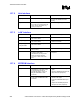
SIN & SOUT Should be daisy-chained between
RIMM connectors:
• MCH SIO pin connects to 1
st
RIMM
connector SIN (B36)
• SOUT (A36) on 1
st
RIMM connector
connects to 2
nd
RIMM connector SIN
(B36)
• A 2.2 kΩ–10 kΩ terminating resistor,
tied to GND, is required on the last
RIMM connector’s SOUT pin.
• Refer to Section 6.1.6.
• Refer to the Rambus datasheets at
http://www.rambus.com
SWE (A57) • If an OEM needs to write to the SPD
devices, it is recommended that this
signal be tied to a GPO pin from
either the ICH2 or the SIO.
• If an OEM does not need to write to
the SPD devices, it is recommended
that this signal be tied to 3.3 V via a
weak pull-up resistor (4.7 k
Ω).
• If SWE = 1, write protected.
• If SWE = 0, not write protected.
• These signals must be driven; do not
leave floating.
• Refer to the RAMBUS datasheets at
http://www.rambus.com
RESET • For the 168-pin RIMM connector, this
is a reserved pin.
• The connector pad is reserved for
future use for the 168-pin RIMM
connector.
• Refer to the RAMBUS datasheets at
http://www.rambus.com
VDD • This is connected to 2.5 V (or 2.5V
SB
)
• It is REQUIRED that the voltage
regulator to the RDRAM* devices
(2.5 V RDRAM device Core) is turned
OFF in S5. This can be
accomplished by connecting the
SLP_S5# signal to the 2.5 V RDRAM
Core voltage regulator.
• It supplies the core voltage for the
RDRAM* technology and interface
logic.
VCMOS • PC600/800/1066:
• This is connected to 1.8 V for
RDRAM technology
• VCMOS must be OFF in S5.
• VCMOS can be generated with a
voltage divider consisting of a 36
Ω
pull-up resistor to VCC2_5 and 100
Ω
resistor to GND.
• S5 is a suspend state and power is
removed from some components on
the motherboard. Therefore, V
CMOS
should be off while in suspend state.
• Refer to Section 6.1.5.