
Intel Pentium 4 Processor in the 478-pin Package / Intel 850 Chipset Platform Family Design Guide

Layout Review Checklist
R
Intel
®
Pentium
®
4 Processor / Intel
®
850 Chipset Family Platform Design Guide 279
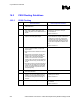
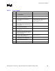
16.3.3 V
term
Layout
√ Recommendations Reason/Impact
• Solid V
TERM
island is on top routing layer; do
not split this plane
• Ground island (for ground side of V
TERM
capacitors) is on top routing layer
• Termination resistors connect directly to the
V
TERM
island on the top routing layer
(without vias)
• Resistor packs are acceptable; however,
discrete resistors are recommended for
increase margin and control.
• Refer to Section 6.1.3.
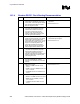
• Decoupling capacitors connect to top layer
V
TERM
island and top routing layer ground
island directly.
• Use at least 2 vias per decoupling capacitor
in the top layer ground island.
• Use 2x100 µF Tantalum capacitors to
decouple V
TERM
.
• Refer to Section 6.1.3.
• Hi-frequency decoupling capacitors must be
spread-out across the termination island so
that all termination resistors are near high
frequency capacitors.
• Refer to Section 6.1.3.
• 100 µF Tantalum capacitor should be at
each end of the V
TERM
island.
• Refer to Section 6.1.3.
• 100 µF Tantalum capacitors must be
connected to the V
TERM
island directly
• Refer to Section 6.1.3.
• 100 µF Tantalum capacitors must have at
least 2 vias/capacitor to ground.
• V
TERM
island should be at least 50 mils wide • Refer to Section 6.1.3