
Intel Pentium 4 Processor in the 478-pin Package / Intel 850 Chipset Platform Family Design Guide


Layout Review Checklist
R
282 Intel
®
Pentium
®
4 Processor / Intel
®
850 Chipset Family Platform Design Guide
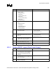
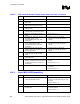
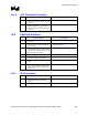
16.3.6 Rambus DRCG* (CTM/CTM# Output Network Layout)
√ Recommendations Reason/Impact
• Series resistors (39 Ω) should be mounted
very near CTM/CTM# pins. Parallel
resistors (51
Ω) should be very near series
resistors.
• Refer to Section 4.3.5.
• CTM/CTM# should be 18 mils wide from the
CTM/CTM# pins to the resistors
• Refer to Section 4.3.3.1.
• CTM/CTM# should be 14 on 6 routed
differential as soon as possible after the
resistor network. When not 14 on 6, the
clocks should be 18 mils wide
• Ensure CTM/CTM# are ground referenced
and the ground reference is connected to
the ground plane every ½ inch to 1 inch with
vias.
• Ensure CTM/CTM# are ground isolated
and the ground isolation is connected to the
ground plane every ½ inch to 1 inch with
vias.
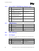
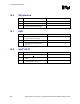
16.3.7 RAMREF Routing
√ Recommendations Reason/Impact
• Ensure 1 x 0.1 µF capacitor on V
REF
at each
RIMM connector
• Refer to Section 6.1.4.
• Use 10-mil wide trace. • Refer to Section 6.1.4.
• Do not route V
REF
near high-speed signals
• V
REF
minimum trace spacing should be
25 mils.
• To reduce crosstalk and maintain signal
integrity.
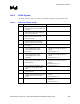
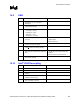
16.4 AGP Guidelines
16.4.1 All 1X Signals
The 1X signals are: CLK, RBF#, WBF#, ST [2:0], PIPE, REQ#, GNT#, PAR, FRAME#, IRDY#,
TRDY, STOP# and DEVSEL#.
√ Recommendations Reason/Impact
• Max trace length 7.5 inches • Refer to Section 7.1.1.
• 5mil trace width, 5 mil trace separation • Refer to Section 7.1.1.
• No trace matching requirements for 1X
signals.
• Refer to Section 7.1.1.