
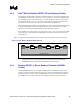
Intel Pentium 4 Processor in the 478-pin Package / Intel 850 Chipset Platform Family Design Guide

Platform Clock Routing Guidelines
R
Intel
®
Pentium
®
4 Processor / Intel
®
850 Chipset Family Platform Design Guide 43
EMI constraints
Clocks are a significant contributor to EMI and should be treated with care. Following these
recommendations can aid in EMI reduction:
• Route clocks on inner layers.
• On internal signals layers maintain a minimum of 100 mils from the edge of the clock traces to
the edge of the system board.
• Maintain uniform spacing between the two halves of differential clocks
• Route clocks on a physical layer adjacent to the VSS reference plane only
• Spread spectrum clocking (SSC) should be enabled to reduce the magnitude of EMI.
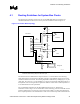
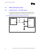
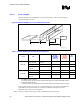
Table 5 describes the routing guidelines for the bus clock signals.
Table 5. BCLK [1:0] Routing Guidelines
Layout Guideline Value Illustration Notes
BCLK Skew between agents 400 ps total
Budget:
150 ps for Clock driver
250 ps for interconnect
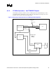
Figure 12 1, 2, 3, 4
Differential pair spacing 7.0 mils Figure 15 5, 6
Spacing to other traces 20 mils Figure 15 —
Line width 7.0 mils Figure 15 7
System board Impedance –
Differential
100 Ω — 8
System board Impedance – single
ended
50 Ω ±15% — 9
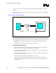
Processor routing length –
L1, L1': Clock driver to Rs
0.5 inches max Figure 13 12
Processor routing length –
L2, L2': Rs to Rs-Rt node
0 – 0.2 inches Figure 13 12
Processor routing length –
L3: RS-RT node to Rt
0 – 0.2 inches Figure 13 12
Processor routing length –
L4, L4': RS-RT Node to Load
0 – 12 inches Figure 13
MCH routing length –
L1: Clock Driver to RS
0.5 inches max Figure 13 12
MCH routing length –
L2, L2': Rs to Rs-Rt node
0 – 0.2 inches Figure 13 12
MCH routing length –
L3: RS-RT node to Rt
0 – 0.2 inches Figure 13 12
MCH routing length –
L4, L4': RS-RT Node to Load
0 – 12 inches Figure 13