
Intel Pentium 4 Processor in the 478-Pin Package Thermal Design Guidelines


Intel
®
Pentium
®
4 Processor in the 478-Pin Package Thermal Design Guidelines
R
Design Guide 33
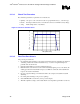
length of time that the clocks are disabled remains constant, and the time period that the clocks are
enabled is adjusted to achieve the desired ratio. For example, if the clock disable period is 3 µs,
and a duty cycle of ¼ (25%) is selected, the clock on time would be reduced to approximately 1 µs
[on time (1 µs) ÷ total cycle time (3 + 1) µs = ¼ duty cycle]. Similarly, for a duty cycle of 7/8
(87.5%), the clock on time would be extended to 21 µs [21 ÷ (21 + 3) = 7/8 duty cycle].
In a high temperature situation, if the thermal control circuit and ACPI MSRs (automatic and on-
demand modes) are used simultaneously, the fixed duty cycle determined by automatic mode
would take precedence.
2.4.4 System Considerations
The Thermal Monitor feature may be used in a variety of ways, depending upon the system design
requirements and capabilities. Intel requires the Thermal Monitor and thermal control circuit to
be enabled for all Intel
®
Pentium
®
4 processor in the 478-pin package based systems. At a
minimum, the thermal control circuit supplies an added level of protection against processor over-
temperature failure.
To minimize the cost of a processor thermal solution, system designers are encouraged to take
advantage of the Thermal Monitor feature capability. The Thermal Monitor feature allows
processor thermal solutions to design to the thermal design power (TDP) target, as opposed to
maximum processor power consumption. Designing to the lower TDP target results in a lower
thermal solution cost, while still maintaining a level of processor performance that is virtually
indistinguishable from systems designed to manage maximum power dissipation levels.
Each application program has its own unique power profile, although the profile has some
variability due to loop decisions, I/O activity and interrupts. In general, compute intensive
applications with a high cache hit rate dissipate more processor power than applications that are
I/O intensive or have low cache hit rates.
The processor thermal design power (TDP) is based on measurements of processor power
consumption while running various high power applications. This data is used to determine those
applications that are interesting from a power perspective. These applications are then evaluated in
a controlled thermal environment to determine their sensitivity to activation of the thermal control
circuit. This data is used to derive the TDP targets published in the processor datasheet.
A system designed to meet the TDP and T
C
targets published in the processor datasheet greatly
reduces the probability of real applications causing the thermal control circuit to activate under
normal operating conditions. Systems that do not meet these specifications could be subject to
more frequent activation of the thermal control circuit depending upon ambient air temperature
and application power profile. Moreover, if a system is significantly under designed, there is a risk
that the Thermal Monitor feature will not be capable of maintaining a safe operating temperature
and the processor could shutdown and signal THERMTRIP#.
For information regarding THERMTRIP#, refer to Section 2.4.6.2 and to the processor datasheet.