
Intel Pentium 4 Processor in the 478-PinPackage at 1.40 GHz, 1.50 GHz, 1.60 GHz, 1.70 GHz, 1.80 GHz, 1.90 GHz, and 2GHz

Electrical Specifications
12 Datasheet
Failure to do so can result in timing violations or reduced lifetime of the component. For
further information and design guidelines, refer to Tab l e 1 for the appropriate Platform
Design Guide, and the Intel® Pentium® 4 Processor VR-Down Design Guidelines.
2.3.1 V
CC
Decoupling
Regulator solutions need to provide bulk capacitance with a low Effective Series
Resistance (ESR) and keep a low interconnect resistance from the regulator to the socket.
Bulk decoupling for the large current swings when the part is powering on, or entering/
exiting low power states, must be provided by the voltage regulator solution (VR). For
more details on this topic, refer to Tab le 1 for the appropriate Platform Design Guide, and
the Intel® Pentium® 4 Processor VR-Down Design Guidelines.
2.3.2 System Bus AGTL+ Decoupling
The Pentium 4 processor in the 478-pin package integrates signal termination on the die
as well as incorporates high frequency decoupling capacitance on the processor package.
Decoupling must also be provided by the system motherboard for proper AGTL+ bus
operation. For more information, refer to Tab le 1 for the appropriate Platform Design
Guide.
2.3.3 System Bus Clock (BCLK[1:0]) and Processor Clocking
BCLK[1:0] directly controls the system bus interface speed as well as the core frequency
of the processor. As in previous generation processors, the Pentium 4 processor in the
478-pin package core frequency is a multiple of the BCLK[1:0] frequency. The Pentium 4
processor in the 478-pin package bus ratio multiplier will be set at its default ratio during
manufacturing. No jumpers or user intervention is necessary, and the processor will
automatically run at the speed indicated on the package.
Like the Pentium 4 processor in the 423-pin package, the Pentium 4 processor in the 478-
pin package uses a differential clocking implementation. For more information on the
Pentium 4 processor in the 478-pin package clocking refer to the CK00 Clock
Synthesizer/Driver Design Guidelines.
2.4 Voltage Identification
The VID specification for Pentium 4 processor in the 478-pin package is supported by the
Intel® Pentium® 4 Processor VR-Down Design Guidelines. The voltage set by the VID
pins is the maximum voltage allowed by the processor. A minimum voltage is provided in
Tab l e 6 and changes with frequency. This allows processors running at a higher frequency
to have a relaxed minimum voltage specification. The specifications have been set such
that one voltage regulator can work with all supported frequencies.
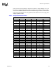
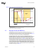
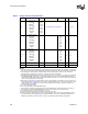
The Pentium 4 processor in the 478-pin package uses five voltage identification pins,
VID[4:0], to support automatic selection of power supply voltages. Table 2 specifies the
voltage level corresponding to the state of VID[4:0]. A ‘1’ in this table refers to a high
voltage level and a ‘0’ refers to low voltage level. The definition provided in Table 2 is not
related in any way to previous P6 processors or VRs, but is compatible with Pentium 4