
Intel Pentium 4 Processor in the 478-PinPackage at 1.40 GHz, 1.50 GHz, 1.60 GHz, 1.70 GHz, 1.80 GHz, 1.90 GHz, and 2GHz

Electrical Specifications
16 Datasheet
TAP, Asynchronous GTL+ inputs, and Asynchronous GTL+ outputs do not include on-die
termination. Input and used outputs must be terminated on the system board. Unused
outputs may be terminated on the system board or left unconnected. Note that leaving
unused output unterminated may interfere with some TAP functions, complicate debug
probing, and prevent boundary scan testing. Signal termination for these signal types is
discussed in the appropriate Platform Design Guide
, and the ITP700 Debug Port Design
Guide.
The TESTHI pins should be tied to the processor V
CC
using a matched resistor, where a
matched resistor has a resistance value within ± 20% of the impedance of the board
transmission line traces. For example, If the trace impedance is 50 Ω,thenavalue
between 40 Ω and 60 Ω is required.
The TESTHI pins may use individual pull-up resistors or be grouped together as detailed
below. A matched resistor should be used for each group:
1) TESTHI[1:0]
2) TESTHI[5:2]
3) TESTHI[10:8]
4) TESTHI[12:11]
Additionally, if the ITPCLKOUT[1:0] pins are not used (refer to Section 5.2) then they may
be connected individually to V
CC
using matched resistors or grouped with TESTHI[5:2]
with a single matched resistor. If they are being used, individual termination with 1 kΩ
resistors is acceptable. Tying ITPCLKOUT[1:0] directly to V
CC
or sharing a pull-up resistor
to V
CC
will prevent use of debug interposers. This implementation is strongly discouraged
for system boards that do not implement an onboard debug port.
As an alternative, group 2 (TESTHI [5:2]), and the ITPCLKOUT[1:0] pins may be tied
directly to the processor V
CC
. This has no impact on system functionality. TESTHI[0] and
TESTHI[12] may also be tied directly to processor V
CC
if resistor termination is a problem,
but matched resistor termination is recommended. In the case of the ITPCLKOUT[1:0],
direct tie to V
CC
is strongly discouraged for system boards that do not implement an
onboard debug port.
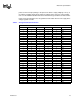
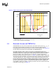
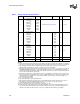
2.6 System Bus Signal Groups
In order to simplify the following discussion, the system bus signals have been combined
into groups by buffer type. AGTL+ input signals have differential input buffers, which use
GTLREF as a reference level. In this document, the term "AGTL+ Input" refers to the
AGTL+ input group as well as the AGTL+ I/O group when receiving. Similarly, "AGTL+
Output" refers to the AGTL+ output group as well as the AGTL+ I/O group when driving.
With the implementation of a source synchronous data bus comes the need to specify two
sets of timing parameters. One set is for common clock signals which are dependent upon
the rising edge of BCLK0 (ADS#, HIT#, HITM#, etc.) and the second set is for the source
synchronous signals which are relative to their respective strobe lines (data and address)
as well as the rising edge of BCLK0. Asychronous signals are still present (A20M#,
IGNNE#, etc.) and can become active at any time during the clock cycle. Tab l e 3 identifies
which signals are common clock, source synchronous, and asynchronous.