
Intel Pentium 4 Processor in the 478-PinPackage at 1.40 GHz, 1.50 GHz, 1.60 GHz, 1.70 GHz, 1.80 GHz, 1.90 GHz, and 2GHz

Electrical Specifications
Datasheet 17
NOTE:
1. Refer to Section 5.2 for signal descriptions.
2. These AGTL+ signals do not have on-die termination and must be terminated on the system board.
3. In processor systems where there is no debug port implemented on the system board, these signals are used
to support a debug port interposer. In systems with the debug port implemented on the system board, these
signals are no connects.
4. These signal groups are not terminated by the processor. Refer to Section 2.5,theITP700 Debug Port
Design Guide, and the appropriate Platform Design Guide as referenced in Table 1 for termination
requirements and further details.
5. The value of these pins during the active-to-inactive edge of RESET# determine processor configuration
options. See Section 7.1 for details.
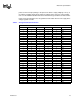
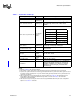
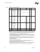
Table 3. System Bus Pin Groups
Signal Group Type Signals
1
AGTL+ Common Clock Input
Synchronous
to BCLK[1:0]
BPRI#, DEFER#, RESET#
2
, RS[2:0]#, RSP#, TRDY#
AGTL+ Common Clock I/O
Synchronous
to BCLK[1:0]
AP[1:0]#, ADS#, BINIT#, BNR#, BPM[5:0]#
2
,BR0#
2
,
DBSY#, DP[3:0]#, DRDY#, HIT#, HITM#, LOCK#,
MCERR#
AGTL+ Source Synchronous I/O
Synchronous
to assoc.
strobe
AGTL+ Strobes
Synchronous
to BCLK[1:0]
ADSTB[1:0]#, DSTBP[3:0]#, DSTBN[3:0]#
Asynchronous GTL+ Input
4, 5
A20M#, IGNNE#, INIT#, LINT0/INTR, LINT1/NMI, SMI#,
SLP#, STPCLK#
Asynchronous GTL+ Output
4
FERR#, IERR#
2
, THERMTRIP#, PROCHOT#
TAP Input
4
Synchronous
to TCK
TCK, TDI, TMS, TRST#
TAP Output
4
Synchronous
to TCK
TDO
System Bus Clock Clock BCLK[1:0], ITP_CLK[1:0]
3
Power/Other
V
CC,VCCA,VCCIOPLL, VID[4:0], VSS,VSSA, GTLREF[3:0],
COMP[1:0], RESERVED, TESTHI[12:8], TESTHI[5:0],
THERMDA, THERMDC, VCC_SENSE, VSS_SENSE,
PWRGOOD, VCCVID, BSEL[1:0], SKTOCC#, DBR
3
,
ITPCLKOUT[1:0]
Signals Associated Strobe
REQ[4:0]#, A[16:3]#
5
ADSTB0#
A[35:17]#
5
ADSTB1#
D[15:0]#, DBI0# DSTBP0#, DSTBN0#
D[31:16]#, DBI1# DSTBP1#, DSTBN1#
D[47:32]#, DBI2# DSTBP2#, DSTBN2#
D[63:48]#, DBI3# DSTBP3#, DSTBN3#