
Intel Pentium 4 Processor in the 478-PinPackage at 1.40 GHz, 1.50 GHz, 1.60 GHz, 1.70 GHz, 1.80 GHz, 1.90 GHz, and 2GHz

Electrical Specifications
Datasheet 19
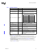
2.10 Maximum Ratings
Table 5 lists the processor’s maximum environmental stress ratings. Functional operation
at the absolute maximum and minimum is neither implied nor guaranteed. The processor
should not receive a clock while subjected to these conditions. Functional operating
parameters are listed in the AC and DC tables. Extended exposure to the maximum
ratings may affect device reliability. Furthermore, although the processor contains
protective circuitry to resist damage from electro static discharge (ESD), one should
always take precautions to avoid high static voltages or electric fields.
NOTE:
1. This rating applies to any processor pin.
2. Contact Intel for storage requirements in excess of one year.
2.11 Processor DC Specifications
The processor DC specifications in this section are defined at the processor core
silicon and not at the package pins unless noted otherwise. See Chapter 5.0 for the
pin signal definitions and signal pin assignments. Most of the signals on the processor
system bus are in the AGTL+ signal group. The DC specifications for these signals are
listed in Table 9.
Previously, legacy signals and Test Access Port (TAP) signals to the processor used low-
voltage CMOS buffer types. However, these interfaces now follow DC specifications
similar to GTL+. The DC specifications for these signal groups are listed in Table 11.
Table 6 through Table 11 list the DC specifications for the Pentium 4 processor in the 478-
pin package and are valid only while meeting specifications for case temperature, clock
frequency, and input voltages. Care should be taken to read all notes associated with
each parameter.
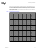
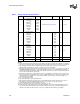
Table 5. Processor DC Absolute Maximum Ratings
Symbol Parameter Min Max Unit Notes
T
STORAGE
Processor storage
temperature
–40 85 °C 2
V
CC
Any processor supply
voltage with respect to V
SS
–0.5 2.10 V 1
V
inAGTL+
AGTL+ buffer DC input
voltage with respect to V
SS
–0.3 2.10 V
V
inAsynch_GTL+
Asynch GTL+ buffer DC
input voltage with respect
to V
SS
–0.3 2.10 V
I
VID
Max VID pin current 5 mA