
Intel Pentium 4 Processor in the 478-PinPackage at 1.40 GHz, 1.50 GHz, 1.60 GHz, 1.70 GHz, 1.80 GHz, 1.90 GHz, and 2GHz

Electrical Specifications
Datasheet 23
NOTES:.
1. Unless otherwise noted, all specifications in this table apply to all processor frequencies.
2. Crossing voltage is defined as the instantaneous voltage value when the rising edge of BCLK0 equals the
falling edge of BCLK1.
3. V
Havg
is the statistical average of the V
H
measured by the oscilloscope.
4. Overshoot is defined as the absolute value of the maximum voltage.
5. Undershoot is defined as the absolute value of the minimum voltage.
6. Ringback Margin is defined as the absolute voltage difference between the maximum Rising Edge Ringback
and the maximum Falling Edge Ringback.
7. Threshold Region is defined as a region entered around the crossing point voltage in which the differential
receiver switches. It includes input threshold hysteresis.
8. The crossing point must meet the absolute and relative crossing point specifications simultaneously.
9. V
Havg
can be measured directly using "Vtop" on Agilent* scopes and "High" on Tektronix* scopes.
10.∆V
CROSS
is defined as the total variation of all crossing voltages as defined in note 2.
NOTES:
1. Unless otherwise noted, all specifications in this table apply to all processor frequencies.
2. VIL is defined as the voltage range at a receiving agent that will be interpreted as a logical low value.
3. VIH is defined as the voltage range at a receiving agent that will be interpreted as a logical high value.
4. V
IH and VOH may experience excursions above V
CC
. However, input signal drivers must comply with the
signal quality specifications in Chapter 3.0.
5. Refer to processor I/O Buffer Models for I/V characteristics.
6. The V
CC
referred to in these specifications is the instantaneous V
CC
.
7. V
OL_MAX
of 0.560 V is guaranteed when driving into a test load of 50 ohms as indicated in Figure 4, with R
TT
enabled.
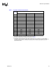
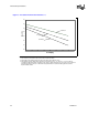
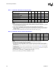
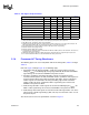
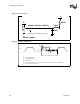
Table 8. System Bus Differential BCLK Specifications
Symbol Parameter Min Typ Max Unit Figure Notes
1
V
L
Input Low Voltage -0.150 0.000 N/A V 6
V
H
Input High Voltage 0.660 0.710 0.850 V 6
V
CROSS(abs)
Absolute Crossing
Point
0.250 N/A 0.550 V 6, 7 2, 3, 8
V
CROSS(rel)
Relative Crossing
Point
0.250 +
0.5(V
Havg
- 0.71)
N/A
0.550 +
0.5(V
Havg
- 0.71)
V 6, 7 2, 3, 8, 9
∆V
CROSS
Range of Crossing
Points
N/A N/A 0.140 V 6, 7 2, 10
V
OV
Overshoot N/A N/A V
H
+0.3 V 6 4
V
US
Undershoot - 0.3 N/A N/A V 6 5
V
RBM
Ringback Margin 0.200 N/A N/A V 6 6
V
TM
Threshold Margin V
CROSS
- 0.100 N/A V
CROSS
+ 0.100 V 6 7
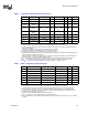
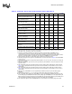
Table 9. AGTL+ Signal Group DC Specifications
Symbol Parameter Min Max Unit Notes
1
VIL Input Low Voltage 0.0 GTLREF - 0.100 V 2, 6
V
IH Input High Voltage GTLREF + 0.100 V
CC
V 3,4,6
V
OH Output High Voltage N/A V
CC
V4,6
I
OL Output Low Current N/A 64 mA 7
I
LI Input Leakage Current N/A ± 100 µA
I
LO Output Leakage Current N/A ± 100 µA
R
ON Buffer On Resistance 5 11 Ω 5