
Intel Pentium 4 Processor in the 478-PinPackage at 1.40 GHz, 1.50 GHz, 1.60 GHz, 1.70 GHz, 1.80 GHz, 1.90 GHz, and 2GHz

Electrical Specifications
24 Datasheet
NOTES:
1. Unless otherwise noted, all specifications in this table apply to all processor frequencies.
2. All outputs are open drain.
3. V
IL
is defined as the voltage range at a receiving agent that will be interpreted as a logical low value.
4. V
IH
is defined as the voltage range at a receiving agent that will be interpreted as a logical high value.
5. V
IH
and V
OH
may experience excursions above V
CC
. However, input signal drivers must comply with the
signal quality specifications in Chapter 3.0.
6. Refer to the processor I/O Buffer Models for I/V characteristics.
7. The V
CC
referred to in these specifications refers to instantaneous V
CC
.
8. The maximum output current is based on maximum current handling capability of the buffer and is not
specified into the test load.
9. V
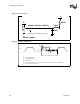
OL_MAX
of 0.560 V is guaranteed when driving into a test load of 50 ohms as indicated in Figure 4, with Rtt
enabled.
NOTES:
1. Unless otherwise noted, all specifications in this table apply to all processor frequencies and cache sizes.
2. All outputs are open drain
3. The TAP signal group must meet the signal quality specifications in Chapter 3.0.
4. Refer to the processor I/O Buffer Models for I/V characteristics.
5. The V
CC
referred to in these specifications refers to instantaneous V
CC
.
6. The maximum output current is based on maximum current handling capability of the buffer and is not
specified into the test load.
7. V
OL_MAX
of 0.360 V is guaranteed when driving into a test load as indicated in Figure 4.
8. V
HYS represents the amount of hysteresis, nominally centered about 1/2 Vcc, for all TAP inputs.
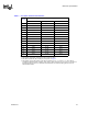
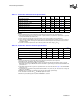
Table 10. Asynchronous GTL+ Signal Group DC Specifications
Symbol Parameter Min Max Unit Notes
1
VIL Input Low Voltage 0.0 GTLREF-0.100 3
V
IH Input High Voltage GTLREF+0.100 V
CC
4, 5, 7
V
OH Output High Voltage V
CC
V 2,5,7
I
OL Output Low Current 64 mA 8, 9
I
LI
Input Leakage Current N/A ± 100 µA
I
LO
Output Leakage Current N/A ± 100 µA
R
ON Buffer On Resistance 5 11 Ω 6
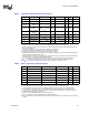
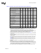
Table 11. PWRGOOD and TAP Signal Group DC Specifications
Symbol Parameter Min Max Unit Notes
1, 2
VHYS Input Hysteresis 200 300 mV 8
V
T+
Input low to high
threshold voltage
1/2 * (V
CC
+VHYS_MIN)1/2*(V
CC
+VHYS_MAX)V 5
V
T-
Input high to low
threshold voltage
1/2 * (V
CC
-VHYS_MAX)1/2*(V
CC
-VHYS_MIN)V 5
VOH Output High Voltage N/A V
CC
V3,5
I
OL Output Low Current 45 mA 6, 7
I
LI
Input Leakage Current ± 100 µA
I
LO
Output Leakage Current ± 100 µA
R
ON Buffer On Resistance 6.25 13.25 Ω 4