
Intel Pentium 4 Processor in the 478-PinPackage at 1.40 GHz, 1.50 GHz, 1.60 GHz, 1.70 GHz, 1.80 GHz, 1.90 GHz, and 2GHz

Electrical Specifications
Datasheet 27
NOTE:
1. Unless otherwise noted, all specifications in this table apply to all processor frequencies and cache sizes.
2. Not 100% tested. Specified by design characterization.
3. All source synchronous AC timings are referenced to their associated strobe at GTLREF. Source
synchronous data signals are referenced to the falling edge of their associated data strobe. Source
synchronous address signals are referenced to the rising and falling edge of their associated address strobe.
All source synchronous AGTL+ signal timings are referenced at GTLREF at the processor core.
4. Unless otherwise noted these specifications apply to both data and address timings.
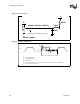
5. Valid delay timings for these signals are specified into the test circuit described in Figure 4 and with GTLREF
at 2/3 V
CC
±2%.
6. Specification is for a minimum swing defined between AGTL+ V
IL_MAX
to V
IH_MIN
. This assumes an edge rate
of 0.3 V/ns to 4.0V/ns.
7. All source synchronous signals must meet the specified setup time to BCLK as well as the setup time to each
respective strobe.
8. This specification represents the minimum time the data or address will be valid before its strobe. Refer to
Ta b le 1 for the appropriate Platform Design Guide for more information on the definitions and use of these
specifications.
9. This specification represents the minimum time the data or address will be valid after its strobe. Refer to
Ta b le 1 for the appropriate Platform Design Guide for more information on the definitions and use of these
specifications.
10.The rising edge of ADSTB# must come approximately 1/2 BCLK period (5 ns) after the falling edge of
ADSTB#.
11. For this timing parameter, n = 1, 2, and 3 for the second, third, and last data strobes respectively.
12.The second data strobe (falling edge of DSTBn#) must come approximately 1/4 BCLK period (2.5 ns) after
the first falling edge of DSTBp#. The third data strobe (falling edge of DSTBp#) must come approximately 2/4
BCLK period (5 ns) after the first falling edge of DSTBp#. The last data strobe (falling edge of DSTBn#) must
come approximately 3/4 BCLK period (7.5 ns) after the first falling edge of DSTBp#.
13.This specification applies only to DSTBN[3:0]# and is measured to the second falling edge of the strobe.
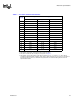
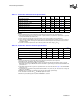
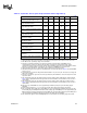
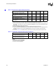
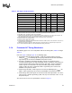
Table 15. System Bus Source Synch AC Specifications AGTL+ Signal Group
T# Parameter Min Typ Max Unit Figure Notes
1,2,3,4
T20: Source Synchronous Data Output
Valid Delay (first data/address only)
0.20 1.20 ns 10, 11 5
T21: T
VBD
: Source Synchronous Data
Output Valid Before Strobe
0.85 ns 11 5, 8
T22: T
VAD
: Source Synchronous Data
Output Valid After Strobe
0.85 ns 11 5, 8
T23: T
VBA
: Source Synchronous Address
Output Valid Before Strobe
1.88 ns 10 5, 8
T24: T
VAA
: Source Synchronous Address
Output Valid After Strobe
1.88 ns 10 5, 9
T25: T
SUSS
: Source Synchronous Input
SetupTimetoStrobe
0.21 ns 10, 11 6
T26: T
HSS
: Source Synchronous Input
Hold Time to Strobe
0.21 ns 10, 11 6
T27: T
SUCC
: Source Synchronous Input
SetupTimetoBCLK[1:0]
0.65 ns 10, 11 7
T28: T
FASS
: First Address Strobe to
Second Address Strobe
1/2 BCLK 10 10
T29: T
FDSS
: First Data Strobe to
Subsequent Strobes
n/4 BCLK 11 11, 12
T30: Data Strobe ‘n’ (DSTBN#) Output
Valid Delay
8.80 10.20 ns 11 13
T31: Address Strobe Output Valid Delay 2.27 4.23 ns 10