
Intel Pentium 4 Processor in the 478-PinPackage at 1.40 GHz, 1.50 GHz, 1.60 GHz, 1.70 GHz, 1.80 GHz, 1.90 GHz, and 2GHz

Pin Listing and Signal Definitions
74 Datasheet
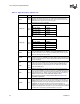
PWRGOOD Input
PWRGOOD (Power Good) is a processor input. The processor requires this
signal to be a clean indication that the clocks and power supplies are stable and
within their specifications. ‘Clean’ implies that the signal will remain low (capable
of sinking leakage current), without glitches, from the time that the power
supplies are turned on until they come within specification. The signal must then
transition monotonically to a high state. Figure 12 illustrates the relationship of
PWRGOOD to the RESET# signal. PWRGOOD can be driven inactive at any
time, but clocks and power must again be stable before a subsequent rising
edge of PWRGOOD. It must also meet the minimum pulse width specification in
Ta b le 16 , and be followed by a 1 to 10 ms RESET# pulse.
The PWRGOOD signal must be supplied to the processor; it is used to protect
internal circuits against voltage sequencing issues. It should be driven high
throughout boundary scan operation.
REQ[4:0]#
Input/
Output
REQ[4:0]# (Request Command) must connect the appropriate pins of all
processor system bus agents. They are asserted by the current bus owner to
define the currently active transaction type. These signals are source
synchronous to ADSTB0#. Refer to the AP[1:0]# signal description for a details
on parity checking of these signals.
RESET# Input
Asserting the RESET# signal resets the processor to a known state and
invalidates its internal caches without writing back any of their contents. For a
power-on Reset, RESET# must stay active for at least one millisecond after V
CC
and BCLK have reached their proper specifications. On observing active
RESET#, all system bus agents will deassert their outputs within two clocks.
RESET# must not be kept asserted for more than 10 ms while PWRGOOD is
asserted.
A number of bus signals are sampled at the active-to-inactive transition of
RESET# for power-on configuration. These configuration options are described
in the Section 7.1.
This signal does not have on-die termination and must be terminated on
the system board.
RS[2:0]# Input
RS[2:0]# (Response Status) are driven by the response agent (the agent
responsible for completion of the current transaction), and must connect the
appropriate pins of all processor system bus agents.
RSP# Input
RSP# (Response Parity) is driven by the response agent (the agent responsible
for completion of the current transaction) during assertion of RS[2:0]#, the
signals for which RSP# provides parity protection. It must connect to the
appropriate pins of all processor system bus agents.
A correct parity signal is high if an even number of covered signals are low and
low if an odd number of covered signals are low. While RS[2:0]# = 000, RSP# is
also high, since this indicates it is not being driven by any agent guaranteeing
correct parity.
SKTOCC# Output
SKTOCC# (Socket Occupied) will be pulled to ground by the processor. System
board designers may use this pin to determine if the processor is present.
SLP# Input
SLP# (Sleep), when asserted in Stop-Grant state, causes the processor to enter
the Sleep state. During Sleep state, the processor stops providing internal clock
signals to all units, leaving only the Phase-Locked Loop (PLL) still operating.
Processors in this state will not recognize snoops or interrupts. The processor
will recognize only assertion of the RESET# signal, deassertion of SLP#, and
removal of the BCLK input while in Sleep state. If SLP# is deasserted, the
processor exits Sleep state and returns to Stop-Grant state, restarting its internal
clock signals to the bus and processor core units. If the BCLK input is stopped
while in the Sleep state the processor will exit the Sleep state and transition to
the Deep Sleep state.
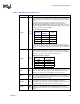
Table 32. Signal Description (Sheet 6 of 8)
Name Type Description