
Intel Pentium 4 Processor in the 478-PinPackage at 1.40 GHz, 1.50 GHz, 1.60 GHz, 1.70 GHz, 1.80 GHz, 1.90 GHz, and 2GHz

Pin Listing and Signal Definitions
Datasheet 75
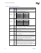
SMI# Input
SMI# (System Management Interrupt) is asserted asynchronously by system
logic. On accepting a System Management Interrupt, the processor saves the
current state and enter System Management Mode (SMM). An SMI
Acknowledge transaction is issued, and the processor begins program execution
from the SMM handler.
If SMI# is asserted during the deassertion of RESET# the processor will tristate
its outputs.
STPCLK# Input
STPCLK# (Stop Clock), when asserted, causes the processor to enter a low
power Stop-Grant state. The processor issues a Stop-Grant Acknowledge
transaction, and stops providing internal clock signals to all processor core units
except the system bus and APIC units. The processor continues to snoop bus
transactions and service interrupts while in Stop-Grant state. When STPCLK# is
deasserted, the processor restarts its internal clock to all units and resumes
execution. The assertion of STPCLK# has no effect on the bus clock; STPCLK#
is an asynchronous input.
TCK Input
TCK (Test Clock) provides the clock input for the processor Test Bus (also known
as the Test Access Port).
TDI Input
TDI (Test Data In) transfers serial test data into the processor. TDI provides the
serial input needed for JTAG specification support.
TDO Output
TDO (Test Data Out) transfers serial test data out of the processor. TDO
provides the serial output needed for JTAG specification support.
TESTHI[12:8]
TESTHI[5:0]
Input
TESTHI[12:8] and TESTHI[5:0] must be connected to a V
CC
power source
through a resistor for proper processor operation. See Section 2.5 for more
details.
THERMDA Other Thermal Diode Anode. See Section 7.3.1.
THERMDC Other Thermal Diode Cathode. See Section 7.3.1.
THERMTRIP# Output
Assertion of THERMTRIP# (Thermal Trip) indicates the processor junction
temperature has reached a level beyond which permanent silicon damage may
occur. Measurement of the temperature is accomplished through an internal
thermal sensor which is configured to trip at approximately 135°C. Upon
assertion of THERMTRIP#, the processor will shut off its internal clocks (thus
halting program execution) in an attempt to reduce the processor junction
temperature. To protect the processor, its core voltage (VCC) must be removed
following the assertion of THERMTRIP#. See Figure 13 and Tab l e 16 for the
appropriate power down sequence and timing requirements. Once activated,
THERMTRIP# remains latched until RESET# is asserted. While the assertion of
the RESET# signal will de-assert THERMTRIP# , if the processor’s junction
temperature remains at or above the trip level, THERMTRIP# will again be
asserted after RESET# is de-asserted.
TMS Input
TMS (Test Mode Select) is a JTAG specification support signal used by debug
tools.
TRDY# Input
TRDY# (Target Ready) is asserted by the target to indicate that it is ready to
receive a write or implicit writeback data transfer. TRDY# must connect the
appropriate pins of all system bus agents.
TRST# Input
TRST# (Test Reset) resets the Test Access Port (TAP) logic. TRST# must be
driven low during power on Reset. This can be done with a 680 Ω pull-down
resistor.
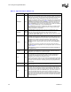
V
CCA
Input
V
CCA
provides isolated power for the internal processor core PLLs. Refer to the
appropriate Platform Design Guide for complete implementation details.
V
CCIOPLL
Input
V
CCIOPLL
provides isolated power for internal processor system bus PLLs. Follow
the guidelines for V
CCA
, and refer to the appropriate Platform Design Guide for
complete implementation details.
Table 32. Signal Description (Sheet 7 of 8)
Name Type Description