
Intel Pentium 4 Processor VR-Down Design Guidelines
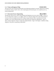
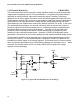
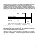
Table Of Contents
- Output Requirements
- Voltage and Current REQUIRED
- Voltage Tolerance REQUIRED
- Load Line Definitions REQUIRED
- Processor Electrical And Thermal Current Support EXPECTED
- No-Load Operation EXPECTED
- Turn-on Response Time PROPOSED
- Processor Power Sequencing REQUIRED
- Overshoot at Turn-On or Turn-Off REQUIRED
- Converter Stability REQUIRED
- Thermal Monitoring PROPOSED
- Input Voltage and Current
- Control Inputs REQUIRED
- Power Good Output (PWRGD) PROPOSED
- Efficiency PROPOSED
- Fault Protection
Intel
®
Pentium
®
4 Processor VR-Down Design Guidelines
15
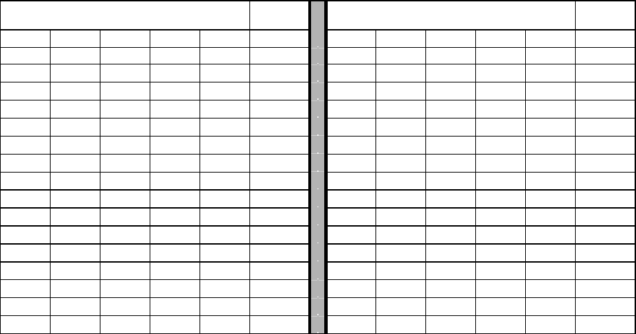
Table 4, Voltage Identification (VID)
Processor Pins (0 = low, 1 = high) Vcc Processor Pins (0 = low, 1 = high) Vcc
VID4 VID3 VID2 VID1 VID0 (VDC) VID4 VID3 VID2 VID1 VID0 (VDC)
1 1 1 1 1 Of
f
0111 1 1.475
1 1 1 1 0 1.1 0111 0 1.5
1 1 1 0 1 1.125 0110 1 1.525
1 1 1 0 0 1.15 0110 0 1.55
1 1 0 1 1 1.175 0101 1 1.575
1 1 0 1 0 1.2 0101 0 1.6
1 1 0 0 1 1.225 0100 1 1.625
1 1 0 0 0 1.250 0100 0 1.65
1 0 1 1 1 1.275 0011 1 1.675
1 0 1 1 0 1.3 0011 0 1.7
1 0 1 0 1 1.325 0010 1 1.725
1 0 1 0 0 1.35 0010 0 1.75
1 0 0 1 1 1.375 0001 1 1.775
1 0 0 1 0 1.4 0001 0 1.8
1 0 0 0 1 1.425 0000 1 1.825
1 0 0 0 0 1.45 0000 0 1.85
4 Power Good Output (PWRGD) PROPOSED
The VR should provide an open collector PWRGD signal consistent with TTL DC levels. On power-
up the PWRGD signal remains in the low-impedance state until the output voltage has stabilized, and
transition to the open (>100kΩ) state within 10 milliseconds of the output voltage stabilizing within
the range specified in Section 1.3. After the output voltage has stabilized, the signal should be in the
low-impedance (to ground) state whenever Vcc
is outside of the required range below and be in the
open state whenever Vcc is within its specified range.
This output should be capable of sinking up to 4mA, while maintaining a voltage of 0.4V or lower.
When the output is in the open state it should be capable of withstanding up to 3.3V. Latch-up or
damage cannot occur if the pull-up voltage on the system board is present with no +12V input present.
The maximum PWRGD voltage should be the maximum Vcc specified in Section 1.3 plus margin to
prevent false de-assertion, but never higher than VID plus 250 mV.
The minimum voltage at which PWRGD is asserted should be the minimum Vcc specified in Section
1.3, minus margin to prevent false de-assertion, but at least 95% of (VID minus 175mV).
VR PWRGD should remain low if the Output Enable control disables the VR.
Please refer to Section 1.7 for power up timing requirements.
5 Efficiency PROPOSED
The efficiency of the VR should be greater than 80% at maximum output current and input voltage. It
should not dissipate more power under any load condition than it does at maximum output current and
maximum input voltage.