
Intel Pentium 4 Processor VR-Down Design Guidelines
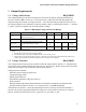
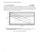
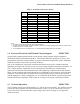
Table Of Contents
- Output Requirements
- Voltage and Current REQUIRED
- Voltage Tolerance REQUIRED
- Load Line Definitions REQUIRED
- Processor Electrical And Thermal Current Support EXPECTED
- No-Load Operation EXPECTED
- Turn-on Response Time PROPOSED
- Processor Power Sequencing REQUIRED
- Overshoot at Turn-On or Turn-Off REQUIRED
- Converter Stability REQUIRED
- Thermal Monitoring PROPOSED
- Input Voltage and Current
- Control Inputs REQUIRED
- Power Good Output (PWRGD) PROPOSED
- Efficiency PROPOSED
- Fault Protection

Intel
®
Pentium
®
4 Processor VR-Down Design Guidelines
3
Contents
1 Output Requirements......................................................................................................................5
1.1 Voltage and Current REQUIRED .......................................................................................5
1.2 Voltage Tolerance REQUIRED ...........................................................................................5
1.3 Load Line Definitions REQUIRED .....................................................................................6
1.4 Processor Electrical And Thermal Current Support EXPECTED .................................7
1.5 No-Load Operation EXPECTED.........................................................................................7
1.6 Turn-on Response Time PROPOSED .................................................................................8
1.7 Processor Power Sequencing REQUIRED..........................................................................8
1.8 Overshoot at Turn-On or Turn-Off REQUIRED ............................................................10
1.9 Converter Stability REQUIRED........................................................................................10
1.10 Thermal Monitoring PROPOSED...................................................................................12
2 Input Voltage and Current...........................................................................................................14
2.1 Input Voltages REQUIRED ...............................................................................................14
2.2 Load Transient Effects on Input Current EXPECTED ..................................................14
3 Control Inputs
REQUIRED .....................................................................................................14
3.1 Output Enable—(OUTEN).................................................................................................14
3.2 Voltage Identification—(VID [0:4])...................................................................................14
4 Power Good Output (PWRGD) PROPOSED ..........................................................................15
5 Efficiency PROPOSED ................................................................................................................15
6 Fault Protection............................................................................................................................16
6.1 Over Voltage Protection EXPECTED...............................................................................16
6.2 Fuse Protection for Power Input PROPOSED .................................................................16
6.3 Overload Protection EXPECTED......................................................................................16
6.4 Reset After Shutdown PROPOSED...................................................................................16