
Intel Pentium 4 Processor VR-Down Design Guidelines
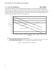
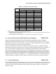
Table Of Contents
- Output Requirements
- Voltage and Current REQUIRED
- Voltage Tolerance REQUIRED
- Load Line Definitions REQUIRED
- Processor Electrical And Thermal Current Support EXPECTED
- No-Load Operation EXPECTED
- Turn-on Response Time PROPOSED
- Processor Power Sequencing REQUIRED
- Overshoot at Turn-On or Turn-Off REQUIRED
- Converter Stability REQUIRED
- Thermal Monitoring PROPOSED
- Input Voltage and Current
- Control Inputs REQUIRED
- Power Good Output (PWRGD) PROPOSED
- Efficiency PROPOSED
- Fault Protection

Intel
®
Pentium
®
4 Processor VR-Down Design Guidelines
5
1 Output Requirements
1.1 Voltage and Current REQUIRED
The voltage regulator for the Intel
®
Pentium
®
4 processor in the 478-pin package and Pentium 4
processor with 512-KB L2 cache on 0.13 micron process is a DC-DC converter that supplies the
required voltage and current to a single processor. A five-bit VID code provided by the processor to
the voltage regulator (VR) determines a reference output voltage, as described in Section 3.1. Sections
1.2 and 1.3 specify deviations from the VID reference voltage.
Table 1, VRD Output Voltage and Current Ratings
Symbol Parameter Processor Minimum Typical Maximum
V
VID
(V) Reference output voltage selected by VID
outputs from processor
1
2
1.750
1.500
V
CC_CORE
(V)
Output voltage measured at Vcc and Vss
pins on solder side of processor socket
See Figure 1 and Table 2
V
MAX
(V) Non-operating (failure) voltage 1
2
2.10
1.75
Icc_max (A) Maximum current the processor draws
during operation
1
2
57.4
70
3
Notes:
1. Intel Pentium 4 processor in the 478-pin package
2. Intel Pentium 4 processor with 512-KB L2 cache on 0.13 micron process
3. Design target covering the load line in Figure 1 and Table 2; each specific motherboard design will have an
output current requirement determined by the processor frequencies it supports.
1.2 Voltage Tolerance REQUIRED
The voltage measured at the processor must be within the range shown in Section 1.3. Measurements
are based on socket voltages measured at processor Vcc and Vss pins. Data in the processor data sheet
always take precedence over the data provided in this document.
Voltage tolerance includes:
− Initial DC output voltage set-point error
− Component aging effects
− Output ripple and noise
− Full ambient temperature range and warm up.
− Static operation
− Dynamic output load changes from minimum-to-maximum or maximum-to-minimum loads
specified in the load lines in section 1.3, as measured over a 100 MHz bandwidth.
The load lines in Section 1.3 show the relationship between Vcc and Icc for the Intel Pentium 4
processor in the 478-pin package and Pentium 4 processor with 512-KB L2 cache on 0.13 micron
process, and also the tolerances from Vcc_typical to Vcc_min and Vcc_max.