
Intel Pentium 4 Processor VR-Down Design Guidelines
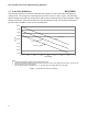
Table Of Contents
- Output Requirements
- Voltage and Current REQUIRED
- Voltage Tolerance REQUIRED
- Load Line Definitions REQUIRED
- Processor Electrical And Thermal Current Support EXPECTED
- No-Load Operation EXPECTED
- Turn-on Response Time PROPOSED
- Processor Power Sequencing REQUIRED
- Overshoot at Turn-On or Turn-Off REQUIRED
- Converter Stability REQUIRED
- Thermal Monitoring PROPOSED
- Input Voltage and Current
- Control Inputs REQUIRED
- Power Good Output (PWRGD) PROPOSED
- Efficiency PROPOSED
- Fault Protection
Intel
®
Pentium
®
4 Processor VR-Down Design Guidelines
6
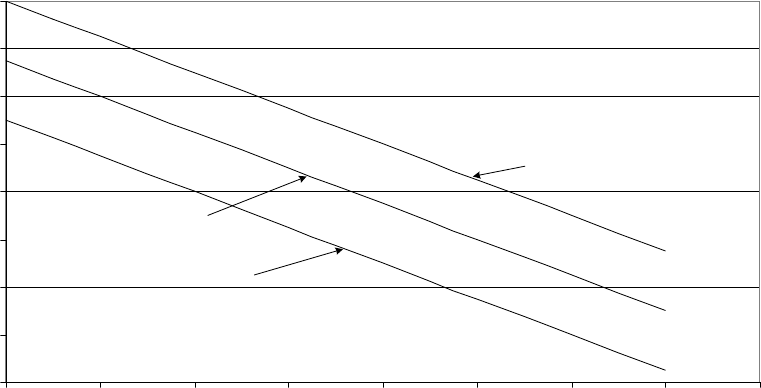
1.3 Load Line Definitions REQUIRED
The following load lines contain DC and transient-droop data, as well as maximum and minimum
voltage levels. The voltages are measured at the processor socket Vcc and Vss pins. The following
figure and table show load-line voltage offsets and current levels based on the VID (maximum) voltage
settings specified in. The load-line slopes are same for Pentium 4 in the 478 Package and Pentium 4
processor with 512-KB L2 cache on 0.13 micron process.
-0.160
-0.140
-0.120
-0.100
-0.080
-0.060
-0.040
-0.020
0.000
0 1020304050607080
Icc Load [A]
Vcc [V]
Vcc Minimum
Vcc Maximum
Vcc Typical
Notes:
1. The load line specification includes both static and transient limits.
2. This load line specification applies to both the Pentium 4 processor in the 478-pin package and the Pentium 4 processor with
512-KB L2 cache on 0.13 micron process.
3. The VID voltage has been normalized to zero; i.e., the graph shows the voltage offset to the VID voltage
Figure 1: Load Line at Processor Socket