
Intel Pentium 4 Processor VR-Down Design Guidelines
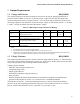
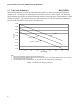
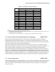
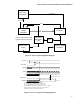
Table Of Contents
- Output Requirements
- Voltage and Current REQUIRED
- Voltage Tolerance REQUIRED
- Load Line Definitions REQUIRED
- Processor Electrical And Thermal Current Support EXPECTED
- No-Load Operation EXPECTED
- Turn-on Response Time PROPOSED
- Processor Power Sequencing REQUIRED
- Overshoot at Turn-On or Turn-Off REQUIRED
- Converter Stability REQUIRED
- Thermal Monitoring PROPOSED
- Input Voltage and Current
- Control Inputs REQUIRED
- Power Good Output (PWRGD) PROPOSED
- Efficiency PROPOSED
- Fault Protection
Intel
®
Pentium
®
4 Processor VR-Down Design Guidelines
8
1.6 Turn-on Response Time PROPOSED
The processor socket voltage should reach its specified range within 50 ms of the input power reaching
its minimum voltage. Please refer to the next paragraph and related figures for complete power up
timing requirements.
1.7 Processor Power Sequencing REQUIRED
The Pentium 4 processor in the 478-pin package and Pentium 4 processor with 512-KB L2 cache on
0.13 micron process require a 1.2V supply to the VCCVID pin to support the on-die VID generation
circuitry. The current requirement for this voltage is approximately 30mA, typically from a linear
regulator. The on-die VID generation circuitry also has power sequencing requirements. Figure 2
shows a block diagram of a power sequencing implementation. Figure 3 and Figure 4 illustrate timing
diagrams of the power sequencing requirements.