
Intel Pentium 4 Processor VR-Down Design Guidelines
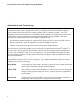
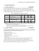
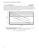
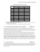
Table Of Contents
- Output Requirements
- Voltage and Current REQUIRED
- Voltage Tolerance REQUIRED
- Load Line Definitions REQUIRED
- Processor Electrical And Thermal Current Support EXPECTED
- No-Load Operation EXPECTED
- Turn-on Response Time PROPOSED
- Processor Power Sequencing REQUIRED
- Overshoot at Turn-On or Turn-Off REQUIRED
- Converter Stability REQUIRED
- Thermal Monitoring PROPOSED
- Input Voltage and Current
- Control Inputs REQUIRED
- Power Good Output (PWRGD) PROPOSED
- Efficiency PROPOSED
- Fault Protection
Intel
®
Pentium
®
4 Processor VR-Down Design Guidelines
9
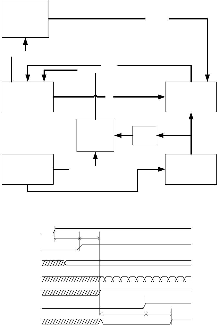
Processor
Voltage
Regulator
System Power
Supply
VCCVID Voltage
Regulator
VID_Good
Generation
Logic
1ms
delay
Processor
VID[4:0]
VID_Good*
PS_PWR_OK
Vcc
*VID_Good connected to voltage
regulator controller output enable
Intel
®
ICH2
Component
PWRGOOD
VRMPWRGD
Figure 2: Power Sequencing Block Diagram
BCLK
Vcc
PWRGOOD
RESET#
VCCVID
VID_GOOD
VID[4:0]
Tc Td
Ta= 1ms minimum (VCCVID > 1V to VID_GOOD high)
Tb= 50ms maximum (VID_GOOD to Vcc valid maximum time)
Tc= T37 (PWRGOOD inactive pulse width) = 10 BCLKs min
Td= T36 (PWRGOOD to RESET# de-assertion time) = 1ms(min), 10ms(max)
Note: VID_GOOD is not a processor signal. This signal is routed to the
output enable pin of the voltage regluator control silicon.
Ta Tb
Figure 3: Power-on Sequence Timing Diagram