
Mobile Intel Pentium 4 Processor - M and Intel 845MP/MZ Chipset Platform Design Guide

Mobile Intel
®
Pentium
®
4 Processor-M and Intel
®
845MP/845MZ Chipset Platform
116 Design Guide
R
9.8. FWH Signaling Voltage Compatibility
Depending on the V_CPU_IO of the processor and the manufacturer of the FWH, there may be signaling
voltage compatibility issues with the ICH3-M. The range of acceptable V_CPU_IO for the ICH3-M is
1.2 V to 2.5 V. If the processor core voltage is not within this range, translation logic will be required on
the processor side before even considering the FWH.
Furthermore, the FWH INIT signal trip points need to be considered because they are NOT consistent
among different FWH manufacturers. The INIT signal is active low. Therefore, the inactive state of the
ICH3-M INIT signal needs to be at a value slightly higher than the V
IH
min FWH INIT pin specification.
The ICH3-M inactive state of this signal is governed by the formula V_CPU_IO - 0.13 V. Therefore if
the V_CPU_IO of the processor is 1.5 V and the V
IH
min spec of the FWH INIT input signal is 1.35 V,
there would be no compatibility issue because 1.5 V - 0.13 V = 1.37 V which is greater than the 1.35 V
minimum of the FWH. If the V
IH
min of the FWH was 1.4 V, then there would be an incompatibility and
logic translation would need to be used. Note that these examples do not take into account noise that
may be encountered on INIT. Care must be taken to ensure that the VIM min specification is met with
ample noise margin.
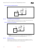
9.8.1. FWH Vpp Design Guidelines
The Vpp pin on the FWH is used for programming the flash cells. The FWH supports Vpp of 3.3 V or 1
2 V. If Vpp is 12 V the flash cells will program about 50% faster than at 3.3 V. However, the FWH only
supports 12 V Vpp for 80 hours. The 12V Vpp would be useful in a programmer environment, which is
typically an event that occurs very infrequently (much less than 80 hours). The VPP pin MUST be tied to
3.3 V on the motherboard.
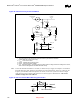
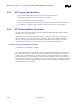
In some instances, it is desirable to program the FWH during assembly with the device soldered down on
the board. In order to decrease programming time it becomes necessary to apply 12 V to the V
PP
pin.
The following circuit will allow testers to put 12 V on the V
PP
pin while keeping this voltage separated
from the 3.3 V plane to which the rest of the power pins are connected. This circuit also allows the
board to operate with 3.3 V on this pin during normal operation.
Figure 58. FWH VPP Isolation Circuitry
1K
FET
12V3.3V
VPP
9.9. RTC
The ICH3-M contains a real time clock (RTC) with 256 bytes of battery backed SRAM. The internal
RTC module provides two key functions: keeping date and time and storing system data in its RAM
when the system is powered down.
The ICH3-M uses a crystal circuit to generate a low-swing, 32-kHz,input sine wave. This input is
amplified and driven back to the crystal circuit via the RTCX2 signal. Internal to the ICH3-M, the