
Mobile Intel Pentium 4 Processor - M and Intel 845MP/MZ Chipset Platform Design Guide

Mobile Intel
®
Pentium
®
4 Processor-M and Intel
®
845MP/845MZ Chipset Platform
130 Design Guide
R
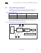
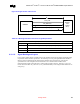
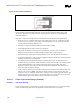
Figure 67. Ground Plane Separation
Separate Chassis Ground Plane
Good grounding requires minimizing inductance levels in the interconnections and keeping ground
returns short, signal loop areas small, and power inputs bypassed to signal return, will significantly
reduce EMI radiation.
Some rules to follow that will help reduce circuit inductance in both backplanes and motherboards.
• Route traces over a continuous plane with no interruptions (don’t route over a split plane). If there
are vacant areas on a ground or power plane, avoid routing signals over the vacant area. This will
increase inductance and EMI radiation levels.
• Separate noisy digital grounds from analog grounds to reduce coupling.
• Noisy digital grounds may affect sensitive DC subsystems.
• All ground vias should be connected to every ground plane; and every power via should be
connected to all power planes at equal potential. This helps reduce circuit inductance.
• Physically locate grounds between a signal path and its return. This will minimize the loop area.
• Avoid fast rise/fall times as much as possible. Signals with fast rise and fall times contain many high
frequency harmonics that can radiate EMI.
• The ground plane beneath the filter/transformer module should be split. The RJ45 and/or RJ11
connector side of the transformer module should have chassis ground beneath it. By splitting ground
planes beneath transformer, noise coupling between the primary and secondary sides of the
transformer and between the adjacent coils in the transformer is minimized. There should not be a
power plane under the magnetic module.
• Create a spark gap between pins 2 through 5 of the Phone line connector(s) and shield ground of 1.6
mm (59.0 mil). This is a
critical requirement needed to past FCC part 68 testing for phone line
connection. Note: For worldwide certification, a trench of 2.5 mm is required. In North America, the
spacing requirement is 1.6 mm. However, home networking can be used in other parts of the world,
including Europe, where some Nordic countries require the 2.5-mm spacing.
9.10.2.3. A Four-Layer Board Design (Example)
9.10.2.3.1. Top Layer Routing
Sensitive analog signals are routed completely on the top layer without the use of vias. This allows tight
control of signal integrity and removes any impedance inconsistencies due to layer changes.