
Mobile Intel Pentium 4 Processor - M and Intel 845MP/MZ Chipset Platform Design Guide

Mobile Intel
®
Pentium
®
4 Processor-M and Intel
®
845MP/845MZ Chipset Platform
132 Design Guide
R
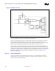
• Use of an 82555 or 82558 physical layer schematic in a PLC design. The transmit terminations and
decoupling are different. There are also differences in the receive circuit. Please follow the
appropriate reference schematic or Ap-Note.
• Not using (or incorrectly using) the termination circuits for the unused pins at the RJ-45/11 and for
the wire-side center-taps of the magnetic modules. These unused RJ pins and wire-side center-taps
must be correctly referenced to chassis ground via the proper value resistor and a capacitance or
termplane. If these are not terminated properly, there can be emissions (FCC) problems, IEEE
conformance issues, and long cable noise (BER) problems. The Ap-Notes have schematics that
illustrate the proper termination for these unused RJ pins and the magnetic center-taps.
• Incorrect differential trace impedances. It is important to have ~100 ohms impedance between the
two traces within a differential pair. This becomes even more important as the differential traces
become longer. It is very common to see customer designs that have differential trace impedances
between 75 ohms and 85 ohms, even when the designers think they've designed for 100 ohms. (To
calculate differential impedance, many impedance calculators only multiply the single-ended
impedance by two. This does not take into account edge-to-edge capacitive coupling between the
two traces. When the two traces within a differential pair are kept close
†
to each other the edge
coupling can lower the effective differential impedance by 5 to 20 ohms. A 10-ohm to 15-ohm drop
in impedance is common.) Short traces will have fewer problems if the differential impedance is a
little off.
• Use of capacitor that is too large between the transmit traces and/or too much capacitance from the
magnetic's transmit center-tap (on the 82562ET side of the magnetic) to ground. Using capacitors
more than a few pF in either of these locations can slow the 100 Mbps rise and fall time so much
that they fail the IEEE rise time and fall time specs. This will also cause return loss to fail at higher
frequencies and will degrade the transmit BER performance. Caution should be exercised if a cap is
put in either of these locations. If a cap is used, it should almost certainly be less than 22 pF. [6 pF
to 12-pF values have been used on past designs with reasonably good success.] These caps are not
necessary, unless there is some overshoot in 100-Mbps mode.
It is important to keep the two traces within a differential pair close
†
to each other. Keeping them close
†
helps to make them more immune to crosstalk and other sources of common-mode noise. This also
means lower emissions (i.e. FCC compliance) from the transmit traces, and better receive BER for the
receive traces.
† Close should be considered to be less than 0.030 inches between the two traces within a differential
pair. 0.007 inch trace-to-trace spacing is recommended.
9.10.3. 82562EH Home/PNA* Guidelines
9.10.3.1. Related Docs
• 82562EH HomePNA* 1 Mb/s Physical Layer Interface – Product Preview Datasheet
• RS-82562EH 1Mb/s Home PNA LAN Connect Option Application Note
Both of the above documents are available at:
http://developer.intel.com/design/network/home/82562eh.htm
For correct LAN performance, designers must follow the general guidelines outlined in Section 9.10.2.
Additional guidelines for implementing an 82562EH Home/PNA* Platform LAN Connect component
are provided below.