
Mobile Intel Pentium 4 Processor - M and Intel 845MP/MZ Chipset Platform Design Guide


Mobile Intel
®
Pentium
®
4 Processor-M and Intel
®
845MP/845MZ Chipset Platform
146 Design Guide
R
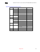
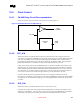
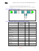
Figure 77. PWRDWN# to CK-408
SLP_S1#
SLP_S3#
PWRDWN#
(CK-408)
V3.3S
NOTES:
1. CK-408 Minimum power up latency should be ≥ 100 µS to guarantee functionality of “AND logic”. In systems
that incorporate any peripherals which are not reset during S3 and which do not use SUS_STAT# as an
indicator of clock validity, ensure that the PWRDWN# pin of the CK-408-compatible clock generator is not
deasserted during S3 entry for a long enough duration such that the system clocks can restart.
2. If platform does not support S1M state, designer may connect SLP_S3 to PWRDWN# pin of CK-408.
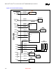
10.3. Clock Group Topology and Layout Routing Guidelines
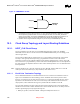
10.3.1. HOST_CLK Clock Group
The clock synthesizer provides four sets of 100-MHz differential clock outputs. The 100-MHz
differential clocks are driven to the Processor the Intel 845MP/845MZ and the processor debug port as
shown in figure below.
The clock driver differential bus output structure is a “Current Mode Current Steering” output which
develops a clock signal by alternately steering a programmable constant current to the external
termination resistors Rt. The resulting amplitude is determined by multiplying IOUT by the value of Rt.
The current IOUT is programmable by a resistor and an internal multiplication factor so the amplitude of
the clock signal can be adjusted for different values of Rt to match impedances or to accommodate future
load requirements.
Note: Designer should use one or the other topologies for CPU, MCH-M, and ITP. Make sure to route all
clocks pairs in the same fashion (layer, layer transition, same number of via).
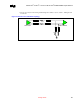
10.3.1.1. End Of Line Termination Topology
The recommended termination for the differential bus clock is a “End of Line Termination.” Refer to
Figure 78 for an illustration of this terminology scheme. Parallel Rt 55-
Ω resistors perform a dual
function, converting the current output of the clock driver to a voltage and matching the driver output
impedance to the transmission line. The series resistors Rs provide isolation from the clock driver’s
output parasitic, which would otherwise appear in parallel with the termination resistor Rt.
The value of Rt should be selected to match the characteristic impedance of the system board and Rs
should be between 20 and 33 Ohms. Simulations have shown that Rs values above 33 Ohms provide no
benefit to signal integrity but only degrade the edge rate.
• Mult0 pin (pin #43) connected to HIGH – making the multiplication factor as 6.