
Mobile Intel Pentium 4 Processor - M and Intel 845MP/MZ Chipset Platform Design Guide


Mobile Intel
®
Pentium
®
4 Processor-M and Intel
®
845MP/845MZ Chipset Platform
150 Design Guide
R
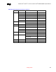
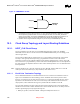
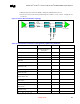
Layout Guideline Value Illustration Notes
driver to Chipset length matching
(L1+L2+L4)
-190 mils
BCLK0 – BCLK1 length matching ± 10 mils --
Rs Series termination value 33 Ω ± 5% 11
Rt Shunt termination value 55 Ω ± 1% (for 55 Ω MB
impedance)
12
NOTES:
1. This number does not include clock driver common m.
2. The skew budget includes clock driver output pair to output pair jitter (differential jitter), and skew, clock skew
due to interconnect process variation, and static skew due to layout differences between clocks to all bus
agents.
3. The interconnect portion of the total budget for this specification assumes clock pairs are routed on multiple
routing layers and routed no longer than the maximum recommended lengths.
4. Skew measured at the load between any two bus agents. Measured at the crossing point.
5. Edge to edge spacing between the two traces of any differential pair. Uniform spacing should be maintained
along the entire length of the trace.
6. Clock traces are routed in a differential configuration. Maintain the minimum recommended spacing between
the two traces of the pair. Do not exceed the maximum trace spacing, as this will degrade the noise rejection of
the network.
7. Set line width to meet correct systemboard impedance. The line width value provided here is a
recommendation to meet the proper trace impedance based on the recommended stackup.
8. The differential impedance of each clock pair is approximately 2*Zsingle-ended*(1-2*Kb) where Kb is the
backwards cross-talk coefficient. For the recommended trace spacing, Kb is very small and the effective
differential impedance is approximately equal to 2 times the single-ended impedance of each half of the pair.
9. The single ended impedance of both halves of a differential pair should be targeted to be of equal value. They
should have the same physical construction. If the BCLK traces vary within the tolerances specified, both
traces of a differential pair must vary equally.
10. Length compensation for the processor socket and package delay is added to chipset routing to match
electrical lengths between the chipset and the processor from the die pad of each. Therefore, the systemboard
trace length for the chipset will be longer than that for the processor. Details of this additional length will be
included in a future revision of the processor package files.
11. Rs values between 20 Ω – 33 Ω have been shown to be effective.
12. Rt shunt termination value should match the systemboard impedance.
13. Minimize L1, L2 and L3 lengths. Long lengths on L2 and L3 degrade effectiveness of source termination and
contribute to ring back.
14. The goal of constraining all bus clocks to one physical routing layer is to minimize the impact on skew due to
variations in Er and the impedance variations due to physical tolerances of circuit board material.
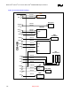
BCLK General Routing Guidelines:
1. When routing the 100-MHz differential clocks do not split up the two halves of a differential clock
pair between layers and route to all agents on the same physical routing layer referenced to ground.
2. If a layer transition is required, make sure that the skew induced by the vias used to transition
between routing layers is compensated in the traces to other agents.
3. Do not place Vias between adjacent complementary clock traces, and avoid differential Vias. Vias
placed in one half of a differential pair must be matched by a via in the other half. Differential
Vias can be placed within length L1, between clock driver and RS, if needed to shorten length L1.
EMI constraints:
• Clocks are a significant contributor to EMI and should be treated with care. Following
recommendations can aid in EMI reduction:
• Maintain uniform spacing between the two halves of differential clocks
Route clocks on physical layer adjacent to the VSS reference plane only