
Mobile Intel Pentium 4 Processor - M and Intel 845MP/MZ Chipset Platform Design Guide

Mobile Intel
®
Pentium
®
4 Processor-M and Intel
®
845MP/845MZ Chipset Platform
156 Design Guide
R
10.3.6. PCICLK Clock Group
The driver is the clock synthesizer 33-MHz clock output buffer and the receiver is the 33-MHz clock
input buffer at the PCI devices on the PCI cards. Note that the goal is to have a maximum of ±1 ns skew
between the clocks within this group, and also a maximum of ±1 ns skew between the clocks of this
group and that of group CLK33.
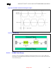
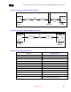
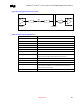
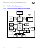
Figure 87. Topology for PCICLK to PCI Device Down
A
R1
Clock
Driver
PCI Device
B
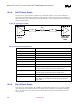
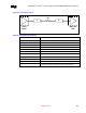
Table 55. PCICLK Routing Guidelines
Parameter Routing Guidelines
Clock Group PCICLK
Topology Point to point
Reference Plane Ground Referenced (Contiguous over entire Length)
Characteristic Trace Impedance (Zo) 60 Ohms ± 15%
Trace Width 5 mils
Trace Spacing 20 mils
Spacing to other traces 20 mils
Trace Length – A Same as CLK33 Trace A
This trace must be exactly length matched to CLK33 Trace A
Trace Length – B Same as CLK33 Trace B
This trace must be exactly length matched to CLK33 Trace B
Resistor R1 = 33 Ohms ± 1%
Skew Requirements Should have a maximum of ±1 ns skew between the clocks within this
group, and also a maximum of
±1 ns skew between the clocks of this
group and that of group CLK33.