
Mobile Intel Pentium 4 Processor - M and Intel 845MP/MZ Chipset Platform Design Guide


Mobile Intel
®
Pentium
®
4 Processor-M and Intel
®
845MP/845MZ Chipset Platform
Design Guide 165
R
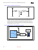
Figure 94. V5REF_Sus Option 1: +V5_Always Not Available in Platform
+V5 or +V5S
+3.3V_Always
USB D+
V5Ref_Sus1
V5Ref_Sus2
USB D-
ICH3-M
USB Power (5V)
GND
Customer specific or
Intel recommended
USB interface
circuits
D2
*
0.1uF
Customer specific or
Intel recommended
USB power circuit
D1
*
D1 and D2 are BAT54 or Equivalent Schottky Diode
11.4.3. MCH-M Power Sequencing Requirements
There are no MCH-M power sequencing requirements. All MCH-M power rails should be stable before
deasserting reset, but the power rails can be brought up in any order desired. Good design practice
would have all MCH-M power rails come up as close in time as practical, with the core voltage (1.5 V)
coming up first.
11.4.4. DDR Power Sequencing Requirements
No DDR-SDRAM power sequencing requirements are specified during power up or power down if the
following criteria are met:
• VDD and VDDQ are driven from a single power converter output.
• VTT is limited to 1.44 V (reflecting VDDQ(max)/2 + 50 mV VREF variation + 40 mV VTT
variation)
• VREF tracks VDDQ/2
• A minimum resistance of 42 Ohm (22 Ohm series resistor + 22 Ohm parallel resistor -5% tolerance)
limits the input current from the VTT supply into any pin.
If the above criteria cannot be met by the system design, then the following table must be adhered to
during power up:
Table 60. Power-up Initialization Sequence (Should Above Listed Requirements Not be Met)
Voltage Description Sequencing Voltage Relationship to Avoid Latch-up
V
DD
Q After or with V
DD
< V
DD
+ 0.3 V
V
TT
After or with V
DD
Q < V
DD
Q + 0.3 V
V
REF
After or with V
DD
Q < V
DD
Q + 0.3 V