
Mobile Intel Pentium 4 Processor - M and Intel 845MP/MZ Chipset Platform Design Guide


Mobile Intel
®
Pentium
®
4 Processor-M and Intel
®
845MP/845MZ Chipset Platform
166 Design Guide
R
11.5. Decoupling Recommendations
Intel recommends proper design and layout of the system board bulk and high frequency decoupling
capacitor solution to meet the transient tolerances for each component. To meet the component transient
load steps, it is necessary to properly place bulk and high frequency capacitors close to the component
power and ground pins.
11.5.1. Transient Response
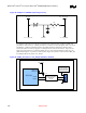
The inductance of the motherboard power planes slows the voltage regulator’s ability to respond quickly
to a current transient. Decoupling a power plane can be broken into several independent parts. The
closer to the load the capacitor is placed the more stray inductance is bypassed. By bypassing the
inductance of leads, power planes, etc., less capacitance is required. However, areas closer to the load
have less room for capacitor placement. Therefore tradeoffs must be made. It is the responsibility of the
system designer to provide adequate high frequency decoupling to manage the highest frequency
components of the current transients. Larger bulk storage capacitors supply current during longer lasting
changes in current demand.
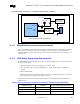
High Frequency decoupling is typically done with ceramic capacitors with a very low ESR. Because of
there low ESR, these capacitors can act very quickly to supply current at the beginning of a transient
event. However, because the ceramic capacitors are small, i.e. they can only store a small amount of
charge, Bulk capacitors are needed too. Bulk capacitors are typically polarized with high capacitance
values and unfortunately higher ESRs. The higher ESR of the Bulk capacitor limits how quickly it can
respond to a transient event. The Bulk and HF capacitors working together can supply the charge needed
to stay in regulator before the regulator can react during a transient. The bulk capacitors and the high
frequency capacitors should be placed as close to the load as possible and in the path of current flow.
Power must be distributed as a plane. This plane can be constructed as an island on a layer used for
other signals, on a supply plane with other power islands, or as a dedicated layer of the PCB. Power
should never be distributed by traces alone. Intel recommends that all layers of the stack-up be used for
power and ground routing.
11.5.2. Processor Decoupling Recommendations
See Processor Power Delivery Design Recommendations.
11.5.3. ICH3-M Decoupling Recommendations
11.5.3.1. 1.8-V Power Supply Rails
Seven 0.1 µF, 0603, X7R capacitors and one 22.0 µF, X5R capacitors should be placed between the
VCCPHL and VCCCORE supply pins and the VSS ground pins. Place the all capacitors as close to the
ICH3-M package as possible, but ensure the 0603 capacitors are the closest to the package. Connections
should be done to minimize loop area and loop inductance of these capacitors.
Eight 0.1
µF, 0603, X7R capacitors and one 22.0 µF, X5R capacitors should be placed between the
VCCPUSB and the VCCPSUS supply pins and the VSS ground pins. Place the all capacitors as close to
the ICH3-M package as possible, but ensure the 0603 capacitors are the closest to the package.
Connections should be done to minimize loop area and loop inductance of these capacitors.