
Mobile Intel Pentium 4 Processor - M and Intel 845MP/MZ Chipset Platform Design Guide


Mobile Intel
®
Pentium
®
4 Processor-M and Intel
®
845MP/845MZ Chipset Platform
168 Design Guide
R
the MCH-M DDR system memory interface and must be placed perpendicular to the MCH-M with the
power (2.5 V) side of the capacitors facing the MCH-M. The trace from the power end of the capacitor
should be as wide as possible and it must connect to a 2.5-V power ball on the outer row of balls on the
MCH-M. Each capacitor should have their 2.5-V via placed directly over and connected to a separate 2.5
V copper finger, and they should be as close to the capacitor pad as possible, within 25 mils. The ground
end of the capacitors must connect to the ground flood and to the ground plane through a via. This via
should be as close to the capacitor pad as possible, within 25mils with as thick a trace as possible.
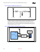
11.5.6. 2.5-V MCH-M System Memory Low Frequency Bulk Decoupling
The MCH-M system memory interface requires low frequency bulk decoupling. Place two 100-µF
electrolytic capacitors between the MCH-M and the first SO-DIMM connector. The power end of the
capacitors must connect to 2.5 V, and the ground end of the capacitors must connect to ground. Also, the
output of the 2.5-V regulator must have enough bulk decoupling to ensure the stability of this regulator.
The amount of bulk decoupling required at the output of the 2.5 V regulator will vary according to the
needs of different OEM design targets.
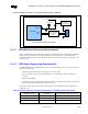
11.5.7. 2.5-V SO-DIMM System Memory High Frequency Decoupling
Discontinuities in the DDR signal return paths will occur when the signals transition between the
motherboard and the SO-DIMMs. To account for this ground to 2.5 V discontinuity, a minimum of nine
0603 0.1 uF high-frequency bypass capacitors are required between the SO-DIMMs to help minimize
any anticipated return path discontinuities that will be created. The bypass capacitors should connect to
2.5 V and ground. The ground trace should connect to a via that transitions to the ground flood and to
the ground plane. The ground via should be placed as close to the ground pad as possible. The 2.5-V
trace should connect to a via that transitions to the 2.5 V copper flood and to the 2.5-V plane. It should
connect to the closet 2.5-V SO-DIMM pin on either the first or second SO-DIMM connector, with a
wide trace. The capacitors 2.5 V traces should be distributed as evenly as possible amongst the two SO-
DIMMs.
11.5.8. 2.5-V SO-DIMM System Memory Low Frequency Decoupling
The DDR SO-DIMMs require low frequency bulk decoupling. Place a total of four 100-µF capacitors,
one at each corner of each SO-DIMM connector. The power end of the capacitors must connect to a 2.5-
V plane, and the ground end of the capacitors must connect to ground plane. The output of the 2.5-V
regulator must have enough bulk decoupling to ensure the stability of the regulator. The amount of bulk
decoupling required at the output of the 2.5-V regulator will vary according to the needs of different
OEM design targets.
11.5.9. 1.25-V DDR VTT High Frequency Decoupling Requirements
The VTT Island must be decoupled using high-speed bypass capacitors, one 0603 0.1-µF capacitor per
two DDR signals. These decoupling capacitors connect directly to the VTT Island and to ground, and
must be spread-out across the termination Island so that all the parallel termination resistors are near
high-frequency capacitors. The capacitor ground via should be as close to the capacitor pad as possible,
within 25 mils with as thick a trace as possible. The ground end of the capacitors must connect to the
ground flood on layer two and to the ground plane on layer three through a via. Finally, the distance
from any DDR termination resistor pin to a VTT capacitor pin must not exceed more then 100 mils.