
Mobile Intel Pentium 4 Processor - M and Intel 845MP/MZ Chipset Platform Design Guide


Mobile Intel
®
Pentium
®
4 Processor-M and Intel
®
845MP/845MZ Chipset Platform
Design Guide 169
R
11.5.10. 1.25-V DDR VTT Low Frequency Bulk Decoupling Requirements
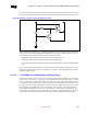
The VTT Termination Island requires low frequency bulk decoupling. Place one 220-µF electrolytic
capacitor at each end of the termination island. The power end of the capacitors must connect to the Vtt
termination island directly, and the ground end of the capacitors must connect to ground. Also, the
output of the 1.25-V regulator must have enough bulk decoupling to ensure the stability of the regulator.
The amount of bulk decoupling required at the output of the 1.25-V regulator will vary according to the
needs of different OEM design targets.
11.5.11. 1.5-V AGP Decoupling
The following routing guidelines are recommended for the optimal system design. The main focus of
these guidelines is to minimize signal integrity problems on the AGP interface of the Intel
845MP/845MZ chipset (MCH-M). The following guidelines are not intended to replace thorough system
validation on Intel 845MP/845MZ chipset-based products.
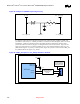
• A minimum of six 0.01-µF capacitors are required and must be as close as possible to the MCH-M.
These should be placed within 70 mils of the outer row of balls on the MCH-M for VDDQ
decoupling. The closer the placement, the better.
• The designer should evenly distribute placement of decoupling capacitors in the AGP interface
signal field.
• Intel recommends that the designer use a low-ESL ceramic capacitor, such as with a 0603 body-type
X7R dielectric.
• In order to add the decoupling capacitors within 70 mils of the MCH-M and/or close to the vias, the
trace spacing may be reduced as the traces go around each capacitor. The narrowing of space
between traces should be minimal and for as short a distance as possible (1-inch max.).
• In addition to the minimum decoupling capacitors, the designer should place bypass capacitors at
vias that transition the AGP signal from one reference signal plane to another. One extra 0.01-
µF
capacitor is required per 10 vias. The capacitor should be placed as close as possible to the center of
the via field.
11.5.12. 1.8-V Hub Interface Decoupling
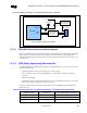
To improve I/O power delivery, use two 0.1-µF capacitors per each component (i.e. the ICH3-M and
MCH-M). These capacitors should be placed within 150 mils from each package, adjacent to the rows
that contain the hub interface. If the layout allows, wide metal fingers running on the VSS side of the
board should connect the +V1.8 side of the capacitors to the +V1.8 power pins. Similarly, if layout
allows, metal fingers running on the +V1.8 side of the board should connect the groundside of the
capacitors to the VSS power pins.
11.5.13. 3.3-V FWH Decoupling
A 0.1-µF capacitor should be placed between the Vcc supply pins and the Vss ground pins to decouple
high frequency noise, which may affect the programmability of the device. Additionally, a 4.7-
µF
capacitor should be placed between the Vcc supply pins and the Vss ground pins to decouple low
frequency noise. The capacitors should be placed no further than 390 mils from the Vcc supply pins.