
Mobile Intel Pentium 4 Processor - M and Intel 845MP/MZ Chipset Platform Design Guide


Mobile Intel
®
Pentium
®
4 Processor-M and Intel
®
845MP/845MZ Chipset Platform
170 Design Guide
R
11.5.14. 3.3-V General LAN Decoupling
• All Vcc pins should be connected to the same power supply.
• All Vss pins should be connected to the same ground plane.
• Four to six decoupling capacitors, including two 4.7-µF capacitors are recommended
• Place decoupling as close as possible to power pins.
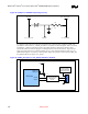
11.6. 3.3-V Clock Driver Decoupling
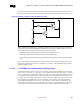
The decoupling caps should be connected taking care to connect the Vdd pins directly to the Vdd side of
the caps. However, the Vss pins should not be connected directly to the Vss side of the caps. Instead they
should be connected to the ground flood under the part that is viaed to the ground plane. This is done to
avoid Vdd glitches propagating out, getting coupled through the decoupling caps to the Vss pins. This
method has been shown to provide the best clock performance.
The decoupling requirements for a CK-408 compliant clock synthesizer are as follows:
• One 10-µf bulk decoupling cap in a 1206 package placed close to the Vdd generation circuitry.
• Six 0.1-µf high frequency decoupling caps in a 0603-package placed close to the Vdd pins on the
Clock driver.
• Three 0.1-µf high frequency decoupling caps in a 0603-package placed close to the VddA pins on
the Clock driver.
• One 10-µf bulk decoupling cap in a 1206-package placed close to the VddA generation circuitry
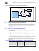
11.7. DDR Power Delivery Design Guidelines
The following sections summarize the DDR system voltage and current requirements as of the release
this document. This document is not the original source for these specifications. For more information
refer to Section 1.1Related Documentation.
The following guidelines are recommended for a MCH-M DDR system memory design. The main focus
of these MCH-M guidelines is to minimize signal integrity problems and improve the power delivery of
the MCH-M system memory interface and the DDR SO-DIMMs.