
Mobile Intel Pentium 4 Processor - M and Intel 845MP/MZ Chipset Platform Design Guide

Mobile Intel
®
Pentium
®
4 Processor-M and Intel
®
845MP/845MZ Chipset Platform
172 Design Guide
R
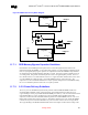
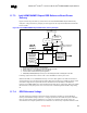
DDR signals and for optimal MCH-M power delivery. The copper fingers must be kept as wide as
possible in order to keep the loop inductance path from the 2.5-V voltage regulator to the MCH-M at a
minimum. In the areas where the copper flooding necks down around the MCH-M make sure to keep
these neck down lengths as short as possible. The 2.5-V copper flooding under the SO-DIMM
connectors must encompass all the SO-DIMM 2.5-V pins and must be solid except for the small areas
where the clocks are routed within the SO-DIMM pin field where they connect to their specified SO-
DIMM pins.
Additionally, a small 2.5-V cooper flood shape should be placed under the MCH-M, to encompass and
increase the copper flooding to the back row of 2.5-V MCH-M pins. This flood must not be placed
under any of the DDR signals. In order to maximize the copper flooding these signals should be kept as
short as possible in order to reduce the amount of serpentining needed in this area on the bottom layer.
Also, a minimum of 12-mil isolation spacing should be maintained between the copper flooding and the
DDR signals. Finally, the six MCH-M 2.5V high frequency decoupling capacitors, located on the top
signal layer, should have their 2.5-V via placed directly over and connected to a separate 2.5-V copper
finger. Refer to Section 11.5 for decoupling capacitors.