
Mobile Intel Pentium 4 Processor - M and Intel 845MP/MZ Chipset Platform Design Guide

Mobile Intel
®
Pentium
®
4 Processor-M and Intel
®
845MP/845MZ Chipset Platform
174 Design Guide
R
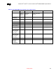
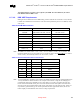
(the top 3 listed) and the MCH-M requirements (next row of 3) and finally the termination voltage and
current requirements.
For convenience, tolerances are given in both % and Volts though validation should be done using the
spec exactly as it is written. The voltage specs are clearly defined under “Specification Definition”. If
this states a tolerance in terms of volts (as Vref says ± 0.050 V) then that specific voltage tolerance
should be used, not the a percentage of the measured value. Likewise, percentages should be used where
stated. If not stated then either way if fine.
Voltage specs are defined as either “Absolute” or “Relative”. These are described below:
Type Of Specification Description
Absolute Specification This is a standard specification most commonly used. This means that
the voltage limits are based on a fixed nominal voltage and have a
symmetric ± tolerance added to determine the acceptable voltage range.
For example, Vdd’s spec does not depend on any other voltage levels. It
is simply 2.5 V ± 8%.
Relative Specification This is a specification whose nominal value is not fixed but is relative to or
is a function of another voltage. This means that the other voltage must
be measured to know what the nominal value is and then the symmetrical
± tolerance added to that measured value. For example, Vref’s spec
depends on the actual value of Vdd to determine Vdd/2 and then
tolerance ±0.050 V from this calculated value.
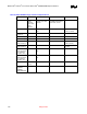
From the table below, it can be seen that only the 2.5-V supply is fixed an absolute specification, whereas
all of the 1.25-V nominal supplies are relative to the 2.5-V supply directly or another 1.25-V supply
which is then relative to the 2.5-V supply. Due to these 1.25-V relative specifications, it becomes very
important that the 1.25-V supply can track the variations in the 2.5V supply and respond according to the
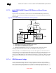
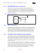
2.5 V variations. This can be implemented as shown in the block diagram in Figure 96 where the 2.5-V
output is divided in half and used to generate the 1.25-V reference into the 1.25-V VR controller design.
In this manner, the 1.25-V VR will respond proportionally to variations in the 2.5-V supply improving
the voltage margin of the relative supply requirements and overall memory system stability.
It should be noted that at launch, all of specifications in this document were current, however it is the
current specifications are considered to be higher than actually expected and will be reduced in future
specifications.