
Mobile Intel Pentium 4 Processor - M and Intel 845MP/MZ Chipset Platform Design Guide

Mobile Intel
®
Pentium
®
4 Processor-M and Intel
®
845MP/845MZ Chipset Platform
180 Design Guide
R
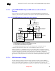
11.7.5. DDR SMRCOMP Resistive Compensation
The MCH-M uses a compensation signal to adjust the system memory buffer characteristics over
temperature, process, and voltage variations. The DDR system memory (SMRCOMP) must be
connected to the DDR termination voltage (1.25 V) through a 30
Ω ±1% resistor and one 0603 0.1-µF
decoupling capacitor to ground. Place the resistor and capacitor as close to the MCH-M as possible,
within 1.0 inch of the MCH-M package. The compensation signal and the VTT trace should be routed
with as wide a trace as possible, minimum of 12-mils wide and isolated from other signals with a
minimum of 10-mils spacing.
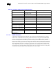
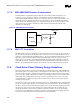
Figure 97. SMRCOMP Recommendation
MCH-M
SMRCOMP
DDR Vtt (1.25 V)
30.1 Ohms
+/- 1%
0.1 uF
Less than 1"
11.7.6. DDR VTT Termination
All DDR signals, except the command clocks, must be terminated to 1.25 V (VTT) using 5% resistors at
the end of the channel opposite the MCH-M. Place a solid 1.25-V (VTT) termination island on the top
signal layer, just beyond the last SO-DIMM connector. The VTT Termination Island must be at least 50-
mils wide. Use this termination island to terminate all DDR signals, using one resistor per signal.
Resistor packs are acceptable, with the understanding that the signals within an RPACK are from the
same DDR signal group. No mixing of signals from different DDR signal groups is allowed within an
RPACK. The parallel termination resistors connect directly to the VTT Island on the top signal layer.
11.8. Clock Driver Power Delivery Design Guidelines
Special care must be taken to provide a quiet VddA supply to the Ref Vdd, VddA and the 48MHz Vdd.
These VddA signals are especially sensitive to switching noise induced by the other Vdd’s on the cock
chip. They are also sensitive to switching noise generated elsewhere in the system such as CPU VRM.
The CLC Pie filter should be designed to provide the best reasonable isolation. Intel recommends that a
solid ground plane be underneath the clock chip on layer 2. (Assuming top trace is layer 1). It is also
recommended that a ground flood be placed directly under the clock chip to provide a low impedance
connection for the Vss pins.
For ALL power connections to planes, decoupling caps and vias , the MAXIMUM trace width allowable
and shortest possible lengths should be used to ensure lowest possible inductance. The decoupling caps
should be connected as shown in the illustration taking care to connect the Vdd pins directly to the Vdd
side of the caps. However the Vss pins should not be connected directly to the Vss side of the caps.
Instead they should be connected to the ground flood under the part that is viaed to the ground plane.
This is done to avoid Vdd glitches propagating out, getting coupled through the decoupling caps to the
Vss pins. This method has been shown to provide the best clock performance.