
Mobile Intel Pentium 4 Processor - M and Intel 845MP/MZ Chipset Platform Design Guide


A
A
B
B
C
C
D
D
E
E
4 4
3 3
2 2
1 1
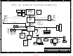
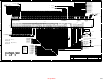
Voltage Rails
STATE SLP_S5#SLP_S1#
OFFLOWS5 / Soft OFF
ON
LOW
OFF
ON
ONLOW OFF
ONHIGH
S4 (Suspend To Disk)
Clocks
ON
ON
LOW
S3 (Suspend to RAM)
SLP_S3# +V*S
ON
LOW
LOW
SIGNAL
HIGH
OFF OFF
HIGH
Full ON
LOW
ON
LOW
HIGH
S1 (Power On Suspend)
LOW OFFON
+V*
Power States
OFF
ONHIGH
HIGH
LOW LOW
ON
+V3ALWAYS
=#
Net Name Suffix
Active Low signal
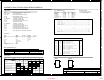
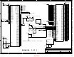
SCHEMATIC ANNOTATIONS AND BOARD INFORMATION
PCI Devices
Device IDSEL # REQ/GNT # Interrupts
Slot 2
Slot 3
A, B, C, D
I C / SMB Addresses
2
Device Address
Clock Generator
Thermal Diode
Bus
Smart Battery
1001 110x
Smart Battery Charger
Smart Selector SMB_SB
SMB_SB
SMB_ICH
SMB_SB
SMB_THRM
PCB Footprints
SOT-23 SOT23-5
1101 001x
0001 011x
0001 001x
0001 010x
Hex
D2
9C
16
12
14
B, C, D, A
C, D, A, B
E, F, G, H
1
2
3
4
5
2
3
1
As seen from top
AD25
AD26
AD27
1
2
3
B, C, D, A4Docking
SO-DIMM0 SMB_ICH
B
A
A
PC/PCI
AGP A, B
1010 0000 A0
AD28
(AD17 internal)
LAN (AD24 internal)
A
USB
Hub to PCI
LPC bridge/IDE/AC97/SMBus
AD29
AD30
AD31
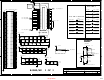
LED Page Ref
Primary IDE.................................24.................................DS27
Secondary IDE...............................24.................................DS24
SMC/KBC NUMLOCK.............................29.................................DS2
SMC/KBC SCROLL LOCK.........................29.................................DS1
SMC/KBC CAPS LOCK...........................29.................................DS3
SW Page Ref
ON/OFF......................................40.................................SW5
LID.........................................29.................................SW3
DIP SWITCH..................................36.................................SW4
Slot 1
SMB_ICHA2SO-DIMM1 1010 0001
1
2
3
DDR Termination:
Address/Command
DATA
Control
1 Series and 1 Parallel
1 Series and 1 Parallel
1 Series and 1 Parallel
MA, BS#, RAS#, CAS#, WE#
DQS, DATA, CB
CKE, CS#
4
Default Jumper Settings
RESET.......................................40.................................SW6
VIRTUAL BATTERY.............................29.................................SW2
SMC/KBC INIT CLOCK..........................24.................................DS26
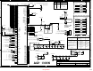
Primary DC system power supply (10 to 17V)
Core voltage for CPU
1.2V For CPU PLL and VID circuitry
DDR Termination voltage
1.5V switched power rail (off in S3-S5)
1.8V always on power rail
1.8V power rail (off in S4-S5)
1.8V switched power rail (off in S3-S5)
2.5V power rail for DDR
3.3V always on power rail
3.3V power rail (off in S4-S5)
3.3V switched power rail (off in S3-S5)
5.0V power rail (off in S4-S5)
5.0V switched power rail (off in S3-S5)
12.0V switched power rail (off in S3-S5)
-12.0V switched power rail for PCI (off in S3-S5)
+VDC
+VCC_CORE
+VCC_VID
+V1.25
+V1.5S
+V1.8ALWAYS
+V1.8
+V1.8S
+V2.5
+V3.3ALWAYS
+V3.3
+V3.3S
+V5
+V5S
+V12S
-V12S
Page
J2 1-X KBC 60/64 DECODE DISABLE 29
J8 1-X INIT CLK DISABLE 30
J11 1-2 KSC DISABLE 29
J12 1-2 LAN PHYCLK Disable 27
J21 2-3 WMT-N/Northwood Select 36
J22 1-X KSC Programming 29
J27 1-X KSC Programming 29
J38 2-3 WMT-N/Northwood Select 36
J49 1-2 SIO Disable 31
J51 1-2 CPU VR Phase num Select 37
J75 1-X CMOS CLEAR 16
J81 2-3 AGP Reset Default 9
Notes and Annotations
242
845MP/MZ Platformm
Title
Sheet of
Project:
212
Design Guide