
Mobile Intel Pentium 4 Processor - M and Intel 845MP/MZ Chipset Platform Design Guide


Mobile Intel
®
Pentium
®
4 Processor-M and Intel
®
845MP/845MZ Chipset Platform
26 Design Guide
R
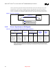
3.2. Processor System Bus (PSB) Routing Guidelines
Table 4 summarizes the layout recommendations for mobile Pentium 4 Processor-M in the 478-pin
package configurations and expands on specific design issues and their recommendations.
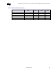
Table 4. System Bus Routing Summary for the Processor
Parameter Processor Routing Guidelines
Line to line spacing Greater than or equal to 2:1 edge-to-edge spacing versus trace to
reference plane height ratio. See Figure 1 for an illustration of this
recommendation.
Data Line lengths (agent to agent spacing) 1.5 inches– 10 inches from - pin to pin. Data signals of the same
source synchronous group should be routed to the same pad-to-pad
length within ± 0.100 inches of the associated strobes. The pad is
defined as the attach point of the silicon die to the package
substrate. Length must be added to the system board to
compensate for package length differences. Signals in the same
source synchronous group should be routed on the same layer and
referenced to Vss.
DSTBn/p[3:0]# A data strobe and its complement should be routed within ±0.025
inches of the same pad-to-pad length. The pad is defined as the
attach point of the silicon die to the package substrate. Length must
be added to the system board to compensate for package length
differences. DSTBn/p# should be routed on the same layer as their
associated data group and referenced to Vss.
Address line lengths(agent to agent spacing) 1.5 inches – 10 inches from pin-to-pin address signals of the same
source synchronous group should be routed to the same Pad-to-
Pad length within± 0.200 inches of the associated strobes. The pad
is defined as the attach point of the silicon die to the package
substrate. Length must be added to the system board to
compensate for package length differences. A layer transition may
occur if the reference plane remains the same (Vss) and the layers
are of the same configuration (all stripline or all microstrip).
ADSTBn/p[1:0]# An address strobe and its complement should be routed within ±
0.200 inches of the same Pad-to-Pad length. The pad is defined as
the attach point of the silicon die to the package substrate. Length
must be added to the system board to compensate for package
length differences. A layer transition may occur if the reference
plane remains the same (Vss) and the layers are of the same
configuration (all stripline or all microstrip).
Common Clock line lengths No length compensation is necessary.
Topology Stripline
Routing priorities All associated signals and strobes should be routed on same layer
for entire length of bus. All signals should be referenced to Vss.
Ideally, layer changes should not occur for any signals. If a layer
change must occur, reference plane must be Vss and the layers
must all be of the same configuration (all stripline or all microstrip
for example).
Clock keepout zones A spacing requirement of 16-20 mils should be maintained around
all clocks.
Trace Impedance 55 ohms ± 15%
Source Synchronous routing restriction There are no length-matching routing restrictions between (or
ithi ) ith th
hdtdd
A