
Mobile Intel Pentium 4 Processor - M and Intel 845MP/MZ Chipset Platform Design Guide


Mobile Intel
®
Pentium
®
4 Processor-M and Intel
®
845MP/845MZ Chipset Platform
Design Guide 27
R
Parameter Processor Routing Guidelines
within) either the source-synchronous data or address groups. As
long as the strobe and associated line length routing guidelines are
met for each group, there is no need to length-match between the
groups. For example, one data group may be routed to the
minimum allowable length while another data group could be routed
to the maximum allowable length. Simulations have verified that the
PSB will still function correctly even under this extreme condition.
Refer to the Intel
®
845MP or 845MZ Chipset Memory Controller Hub Mobile (MCH-M) Datasheet for
MCH-M package dimensions and refer to the Intel
®
Mobile Pentium
®
4 Processor-M in the 478 Pin
Package Signal Integrity Models for Processor package dimensions.
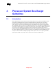
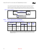
Figure 2. Cross-Sectional View of 2:1 Ratio
2x
x
trace
trace
Reference Plane(Vss)
NOTE: This is the edge-to-edge trace spacing versus trace to reference plane height.
A trace spacing to height above reference plane ratio of 2 to 1 ensures a low crosstalk coefficient. All the
effects of crosstalk are difficult to simulate. The timing and layout guidelines for the Processor have been
created with the assumption of 2:1 trace spacing to height above reference plane ratio. A smaller ratio
would have an unpredictable impact due to crosstalk.
3.2.1. Return Path Evaluation
The return path is the route current takes to return to its source. It may take a path through ground planes,
power planes, other signals, integrated circuits, vias, VRMs etc. Think of the return path as following a
path of least resistance back to the original source. Discontinuities in the return path often have signal
integrity and timing effects that are similar to the discontinuities in the signal conductor. Therefore, the
return paths need to be given similar considerations. A simple way to evaluate return path parasitic
inductance is to draw a loop that traces the current from the driver through the signal conductor to the
receiver, and then back through the ground/power plane to the driver again. The smaller the area of the
loop, the lower the parasitic inductance will be.
The following sets of return path rules apply:
• Always trace out the return current path and provide as much care to the return path as the path of
the signal conductor.
• Decoupling capacitors do not adequately compensate for a plane split.
• Do not allow splits in the reference planes in the path of the return current.
• Do not allow routing of signals on the reference planes near system bus signals.
• Maintain Vss as a reference plane for all system bus signals.
• Do not route over via anti-pads or socket anti-pads.