
Mobile Intel Pentium 4 Processor - M and Intel 845MP/MZ Chipset Platform Design Guide


Mobile Intel
®
Pentium
®
4 Processor-M and Intel
®
845MP/845MZ Chipset Platform
30 Design Guide
R
Source synchronous groups and associated strobes should be routed on the same layer for the entire
length of the bus. This results in a significant reduction of the flight time skew since the dielectric
thickness, line width, and velocity of the signals will be uniform across a single layer of the stackup.
There is no guarantee of a relationship of dielectric thickness, line width, and velocity between layers.
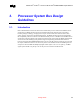
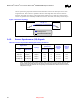
Figure 4. Processor Topology
MCH Processor
Length L1
Package trace
Motherboard PCB trace
Pad Pad
3.4.2. Source Synchronous (SS) Signals
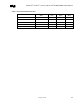
Table 5. Processor System Bus Data Signal Routing Guidelines
Signal Names
Routing Length
(pin-to-pin) L1
CPU
Intel
845MP/845MZ
Topology
Max (inches)
Min
(inches)
Nominal
Impedance
(ohms)
Width &
spacing
(mils)
D[63:0]# HD[63:0]# Stripline 10.0 1.5 55 ±15% 4 & 8
DBI[3:0]# DBI[3:0] Stripline 10.0 1.5 55 ±15% 4 & 8
DSTP[3:0]# HDSTP[3:0]# Stripline 10.0 1.5 55 ± 15% 4 & 8
DSTBN[3:0]# HDSTBN[3:0]# Stripline 10.0 1.5 55 ± 15% 4 & 8
NOTE: The Data signals within each group must be routed to within ± 0.100 inches of its associated “reference”
strobe. The complement strobe must be routed to within ± 0.025 inches of the associate “reference” strobe.
All traces within each signal group must be routed on the same layer (required). Intel recommends that
length of the strobes be centered to the average length of associated data or address traces to maximize
setup/hold time margins.