
Mobile Intel Pentium 4 Processor - M and Intel 845MP/MZ Chipset Platform Design Guide


Mobile Intel
®
Pentium
®
4 Processor-M and Intel
®
845MP/845MZ Chipset Platform
Design Guide 35
R
All signals must meet the AC and DC specifications as documented in the Mobile Intel
®
Pentium
®
Processor-M Datasheet
. In addition, several design guidelines should be implemented when designing
your platform with these signals. They are:
• Although the asynchronous signals are not high frequency in nature, they nevertheless need to be
protected from crosstalk and other sources of noise in the same fashion as the common-clock and
source-synchronous signals. Therefore, the same line-to-line spacing ratio of 2:1. Figure 2 need
also apply.
• Due to the long trace lengths usually associated with these signals, Intel recommends that no
electrical stubs exist and that probing be done at the via nearest to the receiver in order to maintain
signal integrity. These signals should also remain ground-referenced the entire length of the trace.
• If probing is required, active FET probes are recommended as they have a much lower effective
capacitance than passive probes. This, again, is to maintain proper signal integrity and to prevent
any outside influences that may detrimentally affect the system.
• On critical signals, such as DPSLP#, which is used for internal clock control, it may be desirable to
implement additional precautions, such as ground shielding traces or wider keepout zones in order
to assure proper functionality.
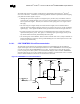
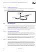
3.4.4.1. CPU THRMTRIP# Circuit Recommendation
The following sections describe the topologies and layout recommendations for the miscellaneous
signals. In the Figure 8 the circuit effectively latches the low state of THRMTRIP# via the D Flip-Flop
once the processor has driven THRMTRIP# to a low state. Operation can be restored if the system
power is cycled (power off/on system). R6 is included if the designer wishes to disable THRMTRIP#
and remove R2, R3, Q1, R4, U1, R1, and R5 and can be included as a no-stuff. Please refer to customer
reference board schematics in Section 13 for all referenced connections.
Figure 8. THRMTRIP# Circuit Recommendation
CLK
D
PRE
CLR
Q
Q
R1
10K
R5
10K
R6
10K
VCC_VID
+V3.3 S
VCC_VIDPWRGD(U13-4)
+V3.3 S
+V3.3 S
H_THRMTRIP#
U11-9
Q1
2N3904
H_THRMTRIP_S#
CPU Ball (A2)
56
Ω
ΩΩ
Ω
R2
R3
10K
R4
10K