
Mobile Intel Pentium 4 Processor - M and Intel 845MP/MZ Chipset Platform Design Guide


Mobile Intel
®
Pentium
®
4 Processor-M and Intel
®
845MP/845MZ Chipset Platform
Design Guide 37
R
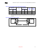
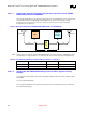
Figure 10. Routing Illustration for LINT1/INTR, LINT0/NMI, DPSLP#, SLP#, STPCLK#, IGNNE#, SMI#
and A20M#
, CPUPERF#, and PWRGOOD- Topology 2, 2A
CPU
ICH3-M
L2
L2
Vtt_CPU
L3
Rtt_CPU
L1
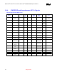
Table 10. Layout Recommendations for Miscellaneous Signals – Topology 2, 2A
L1 L2 L3 Rtt
1.5" - 14.0" 1.1" max 3.0" max Rtt_#2 = 200 ohms ± 5%
Rtt_#2A = 300 ohms ± 5%
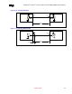
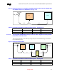
3.4.4.1.3. Topology #2B: PWRGOOD and Asynchronous AGTL+ Signals Driven by ICH3-M
to Both CPU and FWH; INIT#
These signals should adhere to the following routing and layout recommendations. Figure 11 illustrates
the recommended topology.
Figure 11. Routing Illustration INIT#
CPU ICH3-M
Voltage
Translator
Refer to Fig. 12
L2L2
Vtt_CPU
Vcc_FWH
L3L3
Rtt_CPU
Rtt_FWH
L1
FWH
L1
L2
Table 11. Layout Recommendations for Miscellaneous Signals – Topology 2B
L1 L2 L3 Rtt
1.5" - 14.0" 1.1" max 3.0" max Rtt_CPU = 200 Ω ± 5%
Rtt_FWH= 300 Ω ± 5%