
Mobile Intel Pentium 4 Processor - M and Intel 845MP/MZ Chipset Platform Design Guide

Mobile Intel
®
Pentium
®
4 Processor-M and Intel
®
845MP/845MZ Chipset Platform
Design Guide 41
R
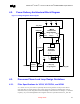
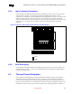
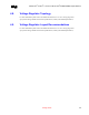
4.2. Power Delivery Architectural Block Diagram
Figure 13. Voltage Regulator Block Diagram
IMVP-III
Processor Core
Voltage Regulator
Mobile Intel®
Pentium® 4
Processor-M
V
CC
VID (1.2V)
Voltage Regulator
V
VID
PWRGOOD_VID
ICH3-M
ChipSet
VR_ON
VR_ON
STP_CPU#
DPRSLPVR
VID[0..4]
V
CC
V
DC
V_5 V_3
V
REF
V
DPRSLP
V
SSA
V
CCA
V
CC
V
TT
VID
LC Filter
V_3
.
.
.
PWRGOOD
CPU_PW RGOOD
4.3. Processor Phase Lock Loop Design Guidelines
4.3.1. Filter Specifications for VCCA, VCCIOPLL, and VSSA
V
CCA
and V
CCIOPLL
are power sources required by the PLL clock generators on the processor silicon.
Since these PLLs are analog in nature, they require quiet power supplies for minimum jitter. Jitter is
detrimental to the system: it degrades external I/O timings as well as internal core timings (i.e., maximum
frequency). To prevent this degradation these supplies must be low pass filtered from VCC_VID
.
The