
Mobile Intel Pentium 4 Processor - M and Intel 845MP/MZ Chipset Platform Design Guide

Mobile Intel
®
Pentium
®
4 Processor-M and Intel
®
845MP/845MZ Chipset Platform
54 Design Guide
R
5. Double Data Rate Synchronous
DRAM (DDR-SDRAM) System
Memory Design Guidelines
5.1. Introduction
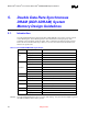
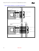
The Intel 845MP/845MZ chipset Double Data Rate (DDR) SDRAM system memory interface consists
of 120 CMOS signals. These CMOS signals have been divided into several signal groups: Data,
Command, Control, Feedback, and Clock signals. Table 13 summarizes the different signal groupings.
Refer to the
Intel
®
845MP/845MZ Chipset Memory Controller Hub-Mobile (MCH-M) Datasheet for
details on the signals listed.
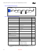
Table 13. Intel 845MP/845MZ DDR Signal Groups
Group Signal Name Description
SDQ[63:0] Data Bus
Data SCB[7:0] Check Bits for ECC Function
SDQS[8:0] Data Strobes
SMA[12:0] Memory Address Bus
SBS[1:0] Bank Select
Command SRAS# Row Address Select
SCAS# Column Address Select
SWE# Write Enable
Control SCKE[3:0] Clock Enable - (One per Device Row)
SCS#[3:0] Chip Select - (One per Device Row)
Feedback RCVENOUT# Output Feedback Signal
RCVENIN# Input Feedback Signal
Clocks SCK[5:0] DDR-SDRAM Differential Clocks - (3 per SO-DIMM)
SCK#[5:0] DDR-SDRAM Inverted Differential Clocks - (3 per SO-DIMM)
Caution: The Intel 845MP/845MZ chipset does not support data masking. The system memory DQM[7:0] pins on
the DDR SO-DIMM’s must be tied to ground.