
Mobile Intel Pentium 4 Processor - M and Intel 845MP/MZ Chipset Platform Design Guide

Mobile Intel
®
Pentium
®
4 Processor-M and Intel
®
845MP/845MZ Chipset Platform
Design Guide 55
R
5.2. DDR System Memory Topology and Layout Design
Guidelines
The Intel 845MP/845MZ chipset Double Data Rate (DDR) SDRAM system memory interface
implements the low swing, high-speed, terminated SSTL_2 topology.
This section contains information and details on the DDR topologies, the DDR layout and routing
guidelines, and the DDR power delivery requirements that will provide for a robust DDR solution on a
Intel 845MP/845MZ based design.
The MCH-M AGP ST[0] signal is sampled by the MCH-M on power-on to indicate at what system
memory mode, DDR, the MCH-M should configure and operate. An internal MCH-M pull-up resistor
on this signal sets the default system memory configuration to PC133 SDRAM. To enable the MCH-M
to operate in DDR mode an external pull-down resistor to ground is required on ST[0]. The
recommended pull-down resistor is 2 KΩ.
The DDR bus has been designed to route in two ground referenced internal layers. DDR System Memory
Topologies for all signal groups have a relatively high via usage, please take this in consideration for the
board layout as the vias and the anti-pad for the via could restrict power delivery to the SO-DIMMs.
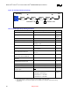
5.2.1. Data Signals – SDQ[63:0], SDQS[8:0], SCB[7:0]
The MCH-M data signals are source synchronous signals that include the 64-bit wide data bus, 8 check
bits for Error Checking and Correction (ECC), and 9 data strobe signals. There is an associated data
strobe (DQS) for each data (DQ) and check bit (CB) group. This section summarizes the DQ/CB to
DQS matching.
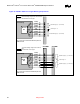
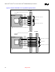
The data signals include SDQ[63:0], SDQS[8:0], and SCB[7:0]. The data signals should transition from
an external layer to an internal signal layer under the MCH-M. Keep to the same internal layer until
transitioning back to an external layer at the series resistor. After the series resistor, the signal route
should transition from the external layer to the same internal layer and route to SO-DIMM0. At SO-
DIMM0 the signal should transition to an external layer and connect to the appropriate pad of the
connector. At the SO-DIMM0 transition continue the signal route on the same internal layer to SO-
DIMM1. Transition back out to an external layer and connect to the appropriate pad of SO-DIMM1 and
the parallel termination resistor.
Data Signals (SDQ[63:0],SDQS[8:0],SCB[7:0]) need to be routed on the same inner signal layer. In
addition, match routing topology and via placement for all signals in a given byte lane including the
associated strobe. External trace lengths should be minimized. To facilitate simpler routing, swapping
of the byte lane and the associated strobe is allowed. Bit swapping within the byte lane is also allowed.
Intel suggests that the parallel termination be placed on both sides of SO-DIMM1 to simplify routing and
minimize trace lengths. All internal and external signals should be ground referenced to keep the path of
the return current continuous. Resistor packs are acceptable for the series (Rs) and parallel (Rt) data and
strobe termination resistors, but data and strobe signals can not be placed within the same R pack as the
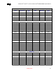
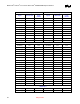
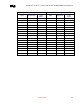
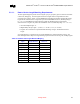
command and control signals. The table and diagrams below depict the recommended topology and
layout routing guidelines for the DDR-SDRAM data signals.