
Mobile Intel Pentium 4 Processor - M and Intel 845MP/MZ Chipset Platform Design Guide

Mobile Intel
®
Pentium
®
4 Processor-M and Intel
®
845MP/845MZ Chipset Platform
56 Design Guide
R
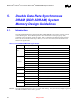
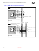
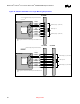
Figure 20. Data Signal Routing Topology
R
t
Rs
SO-DIMM1 PAD
SO-DIMM0 PAD
Vt
t
w
MCH
Pad
MCH Pkg
L1
L2
L3
L4
w
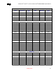
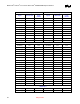
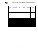
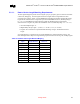
Table 14. Data Signal Group Routing Guidelines
Parameter Routing Guidelines Figure
Signal Group Data – SDQ[63:0], SCB[7:0], SDQS[8:0]
Topology Daisy Chain
Figure 20
Figure 23
Reference Plane Ground Referenced
Characteristic Trace Impedance (Zo) 55 Ω ±15%
Trace Width Inner layer: 4 mils
Outer layer: 5 mils
Trace to space ratio • 1:2 (e.g. 4 mil trace 8 mil space)
Group Spacing Isolation spacing from non-DDR related signals =
20 mils minimum
Trace Length L1– MCH-M die pad to
Series Termination Resistor Pad
Min = 2.0”
Max = 3.5”
Figure 20
Trace Length L2 – Series Termination
Resistor Pad to First SO-DIMM Pad
Max = 0.75” Figure 20
Trace Length L3 – SO-DIMM Pad to SO-
DIMM Pad
Max = 1.25” Figure 20
Trace Length L4 – Last SO-DIMM Pad to
Parallel termination Resistor Pad
Max = 0.8” Figure 20
Series Resistor (Rs) 22 Ω ± 5% (see note below) Figure 20
Termination Resistor (Rtt) 56 Ω ± 5% (see note below) Figure 20
Maximum Recommended motherboard via
Count per signal
5 vias
Length Matching Requirements • SDQ[63:0], SCB[7:0] to SDQS[8:0]
• SDQS[8:0] to SCK/SCK#[5:0]
• See Section 5.2.1.1 for details
• See Section 5.2.1.2 for details
Figure 21,
Figure 22
NOTES:
1. Recommended resistor values may change in a later revision of the design guide.
2. The overall maximum and minimum lengths to the SO-DIMM must comply with clock length matching
requirements.