
Mobile Intel Pentium 4 Processor - M and Intel 845MP/MZ Chipset Platform Design Guide

Mobile Intel
®
Pentium
®
4 Processor-M and Intel
®
845MP/845MZ Chipset Platform
66 Design Guide
R
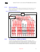
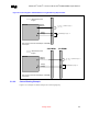
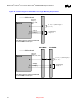
Figure 27. Control Routing Example
Control routing is shown in red. The majority of the control signal route is on an internal layer, both
external layers are used for parallel termination R-pack placement.
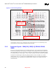
5.2.3. Command Signals – SMA[12:0], SBS[1:0], SRAS#, SCAS#,
SWE#
There are two supported topologies for the command signal group. This section has been divided into
two subsection; Topology 1 and Topology 2. Topology 2 is the topology that best allows for placement
of the SO-DIMMs back to back in the butterfly configuration, thus minimizing the SO-DIMM footprint
area. Mixing topology 1 and topology 2 is “OK”, as long as designer follows this document’s guidelines.
The MCH-M command signals; SMA[12:0], SBS[1:0], SRAS#, SCAS#, and SWE#; are common
clocked signals. They are “clocked” into the DDR SDRAMs using the clock signals SCK/SCK#[5:0].
The MCH-M drives the command and clock signals together, with the clocks crossing in the valid
command window.
FROM MCH-M
Control signals
Parallel Termination on Both
Layers