
Mobile Intel Pentium 4 Processor - M and Intel 845MP/MZ Chipset Platform Design Guide

Mobile Intel
®
Pentium
®
4 Processor-M and Intel
®
845MP/845MZ Chipset Platform
68 Design Guide
R
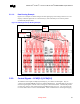
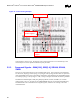
Table 18. Command Signal Group Routing Guidelines
1
Parameter Routing Guidelines Figure
Signal Group Command – SMA[12:0], SBS[1:0], SRAS#,
SCAS#, SWE#
Topology Daisy Chain Figure 28,
Figure 31
Reference Plane Ground Referenced
2
Characteristic Trace Impedance (Zo) 55Ω ±15%
Trace Width Inner layers= 4 mils
Outer layer= 5 mils
Trace to space ratio 1:2 (e.g. 4mil trace 8mil space)
Group Spacing Isolation spacing from non-DDR related signals =
20 mils
Trace Length L1 – MCH-M Command Signal
ball to Rs Pad
Min = 1.0”
Max= 4.0”
Figure 28
Trace Length L2 + L3 – SO-DIMM0 Pad to
Rd2d Pad; Rd2d Pad to SO-DIMM1 pad
Max=1.3” Figure 28
Trace Length L4 – SO-DIMM1 Pad to Rt Pad Max =0.8” Figure 28
Series Resistor (Rd2d) SO-DIMM0 to SO-
DIMM1
10 Ω ± 5% Figure 28
Parallel Termination Resistor (Rt) 56 Ω ± 5% Figure 28
Maximum Recommended motherboard via
Count per signal
5 vias3
Figure 31
Length Matching Requirements CMD to SCK/SCK#[5:0]
See 5.2.3.1.2 for details
Figure 30
NOTES:
1. Recommendation may change in a later revision of the design guide based on a post silicon simulation
analysis.
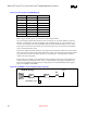
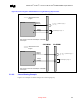
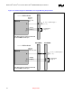
2. Where ever possible command signals should be routed on adjacent layers to the referenced plane. See
Figure 29 below for example, the command signal routing should only route on Signal 1 and Signal 2 layer
where Signal 1 may be external (microstrip) and Signal 2 may be internal (stripline) or where Signal 1 is
internal(stripline) and Signal 2 is external(microstrip). The ground plane is shared between Signal 1 and
Signal2.
3. It is possible to route using 3 vias if one via is shared that connects to SO-DIMM1 and the parallel termination
resistor.
Note: The overall maximum and minimum lengths to the SO-DIMM must comply with clock length matching
requirements.