
Mobile Intel Pentium 4 Processor - M and Intel 845MP/MZ Chipset Platform Design Guide

Mobile Intel
®
Pentium
®
4 Processor-M and Intel
®
845MP/845MZ Chipset Platform
72 Design Guide
R
5.2.3.2. Command Topology 2 Solution
5.2.3.2.1. Routing Description for Command Topology 2
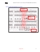
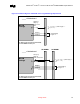
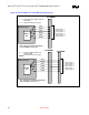
Refer to Figure 32 and Figure 33 for clarification of the description below.
The command signal routing should transition from an external layer to an internal signal layer under the
MCH-M. Keep to the same internal layer until transitioning back to an external layer at the series resistor
Rd2d. At this point there is a T in the topology. One leg of the T will route through Rd2d and either
transition back to the same internal layer or stay external and landing on the appropriate connector pad of
SO-DIMM0. If it was necessary to return to the internal layer the signal should return to the external
layer immediately prior to landing on the appropriate connector pad of SO-DIMM0. The other leg of the
T will continue on the same internal layer and return to the external layer immediately prior to landing on
the appropriate connector pad of
SO-DIMM1. If possible stay on the external layer and connect to the
parallel termination resistor or if the parallel termination resistor is on the opposite side of the board from
the SO-DIMM1 connector then share the via and route to the parallel termination resistor. If sharing the
via or using the opposite side of the board is not possible, continue on the same internal layer and route
to the external layer immediately prior to the termination resistor.
External trace lengths should be minimized. It is suggested that the parallel termination be placed on
both sides of the board to simplify routing and minimize trace lengths. All internal and external signals
should be ground referenced to keep the path of the return current continuous. It is recommended that
command signal group be routed on same internal layer.
Resistor packs are acceptable for the series (Rd2d) and parallel (Rt) command termination resistors but
command signals can’t be placed within the same Rpacks as data, strobe or control signals.
The diagrams and tables below depict the recommended topology and layout routing guidelines for the
DDR-SDRAM command signals going to SO-DIMM0 and SO-DIMM1.
Figure 32. Command Signal Routing Topology
w
SO-DIMM1 PAD
SO-DIMM0 PAD
Vt
t
MCH-M
Pad
MCH-M Package
L1
L3
R
t
Rd2d
L2
L4